

Intel Foundry has released a marketing document, detailing the company's advanced solutions in hardware development and implementation for artificial intelligence applications and high-performance computing. Intel also showcased a "chip prototype for AI," highlighting the company's current capabilities in packaging.
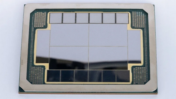
Intel presented a system-in-package (SiP) measuring eight photomasks of standard chips, featuring four logic blocks, 12 HBM4-class stacks, and two input-output units. Unlike the large-scale concept with 16 logic blocks and 24 HBM5 stacks, revealed by the company last month, this system is indeed production-ready today.
It is important to note that Intel Foundry showcased a non-operational AI accelerator, but rather a "chip prototype for AI," illustrating how future processors for AI and high-performance computing can be physically constructed (or rather, assembled). Intel demonstrates the entire construction methodology that integrates large computing blocks, stacks of high-speed memory, ultra-fast inter-chip connections, and new power technologies within a single technology package. This package is significantly different from what companies like TSMC currently offer. Intel aims to show that next-generation processors for high-performance AI can feature a multi-chiplet design, and Intel Foundry is already capable of producing them.
The demonstrated platform is based on four large logical blocks, presumably built on Intel's 18A technology (therefore featuring RibbonFET transistors with a circular gate and a PowerVia power delivery system on the back), which are surrounded by HBM4 class memory stacks and input-output blocks. All key components are presumed to be connected by EMIB-T 2.5D bridges, integrated directly into the package substrate. Intel employs the EMIB-T inter-chiplet interface technology, which adds through-silicon vias within the bridges so that power and signals can flow both vertically and horizontally, maximizing the density of interconnections and power delivery. The platform is designed for UCIe inter-chip interfaces, operating at speeds of 32 GT/s and above, which also appear to be used for connecting C-HBM4E stacks.
The chip test sample also demonstrates Intel's transition to vertical assembly. The company's technology process roadmap includes the Intel 18A-PT technology, specifically developed for chiplets, which imply placing other logic crystals or memory on top. Consequently, chiplets must have back-side power delivery and utilize through and hybrid interconnects. For the 'AI processor test sample,' the base 18A-PT crystals are positioned beneath the 18A/18A-P compute crystals and either function as large cache memory chips or perform another auxiliary function. To achieve vertical chiplet connectivity, Intel employs the Foveros packaging technology family — Foveros 2.5D, Foveros-R, and Foveros Direct 3D. These enable the implementation of fine-pitched copper connections between active crystals to ensure maximum bandwidth and energy efficiency for the upper crystals. Together with the EMIB bridges, these methods allow Intel to create a hybrid lateral-vertical assembly, which the company positions as an alternative to larger silicon interposers with higher wafer utilization and yield.
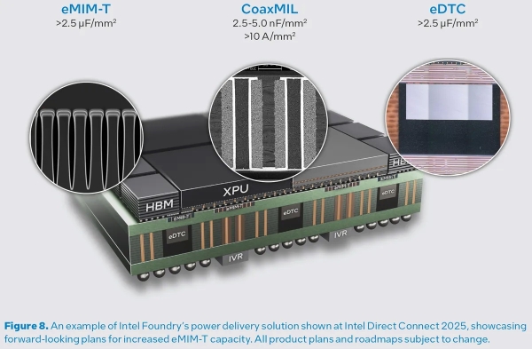
For multi-chiplet AI accelerators and high-performance computing, the primary structural constraint is power delivery. To address this, the Intel platform must integrate all the latest Intel innovations in energy efficiency, including PowerVia, Omni MIM embedded capacitors, bridge decoupling at the EMIB-T level, eDTC and eMIM-T capacitors on the base die, as well as CoaxMIL embedded inductors to support the integrated voltage regulators (IVR) located beneath each stack and under the package itself (unlike the IVR in TSMC's CoWoS-L, which are part of the interposer). This multi-layered network is designed to support stable current in generative AI workloads without a drop in voltage.
With its demonstration, Intel is clearly aiming to attract customers. It's still unknown whether the next-generation AI accelerator code-named Jaguar Shores, set for release in 2027, will utilize the architecture Intel is showcasing today.
Source:
Source: 3dnews.ru
