

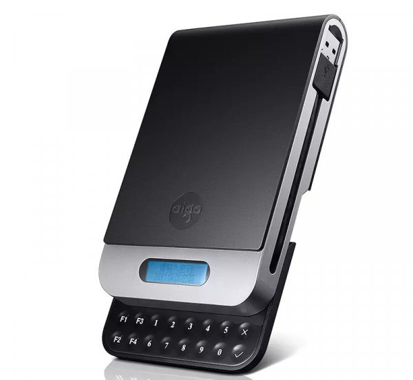
Reversing and hacking external self-encrypting drives has been a long-standing hobby of mine. In the past, I've experimented with models like Zalman VE-400, Zalman ZM-SHE500, and Zalman ZM-VE500. Recently, a colleague brought me another specimen: Patriot (Aigo) SK8671, which is built with a typical design—an LCD indicator and a keyboard for entering the PIN code. Here’s what I came up with…
1. Introduction
Case

Packaging
Access to data stored on the disk, which is supposedly encrypted, is obtained after entering the PIN code. A few introductory remarks about this device:
- To change the PIN code, you need to press F1 before unlocking;
- The PIN code must contain between 6 and 9 digits;
- After 15 incorrect attempts, the disk is wiped.
2. Hardware architecture
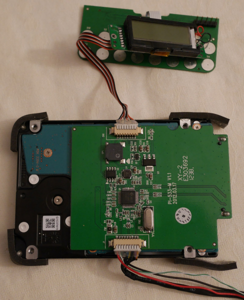
First, we disassemble the device to understand what components it consists of. The most tedious part is opening the case: a lot of microscopic screws and plastic. After opening the case, we see the following (pay attention to the five-pin connector I soldered):
2.1. Mainboard
The mainboard is quite simple:
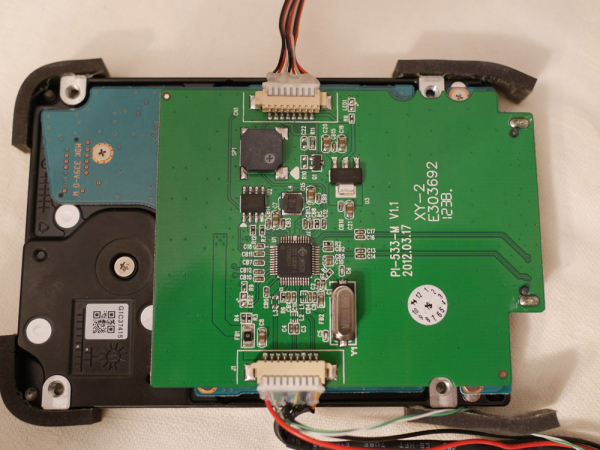
The most notable parts (see top to bottom):
- Connector for the LCD indicator (CN1);
- Buzzer (SP1);
- Pm25LD010 () SPI flash chip (U2);
- Jmicron JMS539 () USB-SATA controller (U1);
- USB 3 connector (J1).
The SPI flash stores firmware for the JMS539 and some settings.
2.2. LCD indicator board
There’s nothing remarkable on the LCD board.
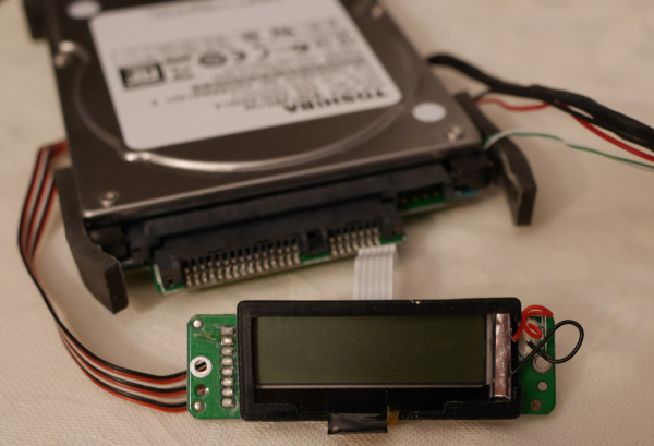
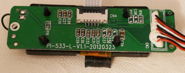
Just:
- LCD indicator of unknown origin (probably from a Chinese font set); with serial control;
- ribbon connector for the keyboard board.
2.3. Keyboard board
Looking at the keyboard board, things take a more interesting turn.
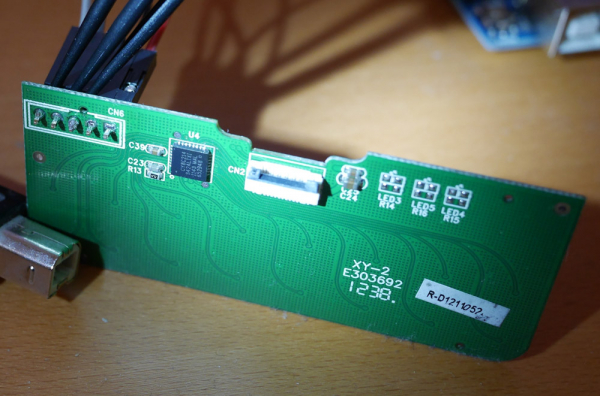
Here, on the back side, we see a ribbon connector, and also a Cypress CY8C21434 – PSoC 1 microcontroller (from now on we’ll just call it PSoC)
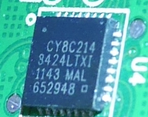
CY8C21434 uses the M8C instruction set (see. ). On the [product page]( () it states that it supports (solution from Cypress for capacitive keyboards). Here you can see the five-pin connector I soldered – this is the standard approach for connecting an external programmer via the ISSP interface.
2.4. Inspecting the wires
Let’s figure out what is connected to what here. It’s enough to check the wires with a multimeter:
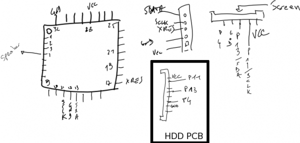
Explanations for this hastily drawn diagram:
- The PSoC is described in the technical specification;
- the next connector, the one on the right – is the ISSP interface, which coincidentally corresponds to what is written about it on the Internet;
- the far right connector – is the terminal for the ribbon connector to the keyboard board;
- the black rectangle – is the schematic of the CN1 connector, intended for connecting the main board with the LCD board. P11, P13, and P4 are connected to the PSoC pins 11, 13, and 4 on the LCD board.
3. Sequence of attack steps
Now that we know what components this storage device consists of, we need to: 1) make sure that the basic encryption functionality is actually present; 2) find out how the encryption keys are generated/saved; 3) locate where the PIN code is verified.
To do this, I took the following steps:
- I dumped the data from the SPI flash;
- I tried to dump the data from the PSoC flash;
- I confirmed that the data exchange between the Cypress PSoC and JMS539 actually includes the pressed keys;
- I made sure that when changing the password, nothing is rewritten in the SPI flash;
- I was too lazy to reverse-engineer the 8051 firmware from JMS539.
3.1. Dumping data from the SPI flash
This procedure is very simple:
- connect the probes to the flash pins: CLK, MOSI, MISO and (optionally) EN;
- sniff the communications with a sniffer using a logic analyzer (I used );
- decode the SPI protocol and export the results to CSV;
- use , to parse the results and obtain the dump.
Note that this approach works particularly well in the case of the JMS539 controller, as this controller loads the entire firmware from the flash during initialization.
$ decode_spi.rb boot_spi1.csv dump
0.039776 : WRITE DISABLE
0.039777 : JEDEC READ ID
0.039784 : ID 0x7f 0x9d 0x21
---------------------
0.039788 : READ @ 0x0
0x12,0x42,0x00,0xd3,0x22,0x00,
[...]
$ ls --size --block-size=1 dump
49152 dump
$ sha1sum dump
3d9db0dde7b4aadd2b7705a46b5d04e1a1f3b125 dump
After extracting the dump from the SPI flash, I concluded that its sole purpose is to store the firmware for the JMicron control device, which is integrated into the 8051 microcontroller. Unfortunately, extracting the SPI flash dump turned out to be useless:
- when changing the PIN code, the flash dump remains the same;
- after the initialization phase, the device does not access the SPI flash.
3.2. Sniffing Communications
This is one way to find out which chip is responsible for checking communications for the time/content of interest. As we already know, the USB-SATA controller is connected to the Cypress PSoC through connector CN1 and two ribbons. So we connect probes to the three corresponding pins:
- P4, general input/output;
- P11, I2C SCL;
- P13, I2C SDA.
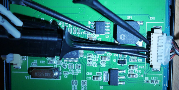
Then we launch the Saleae logic analyzer and type on the keyboard: “123456~”. As a result, we see the following diagram.

In it, we can observe three data exchange channels:
- on channel P4, several short bursts;
- on P11 and P13 – nearly continuous data exchange.
By enlarging the first burst on channel P4 (the blue rectangle from the previous image), we see the following:
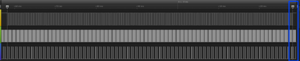
Here we can see that on P4, there is almost 70ms of uniform signal which, at first glance, seemed to act as a synchronization signal. However, after taking some time to verify my hypothesis, I found that this is not a synchronization signal, but an audio stream that is output to the buzzer when keys are pressed. Therefore, this part of the signal itself does not contain any useful information for us. However, it can be used as an indicator to know when the PSoC registers a key press.
However, the last audio stream on channel P4 is somewhat different from the others: it is the sound for the "incorrect PIN code"!
Returning to the key press diagram, when zooming in on the last audio stream (see again the blue rectangle), we obtain:
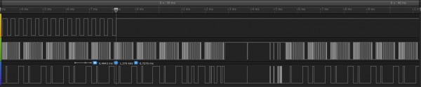
Here we see uniform signals on P11. So it seems this is the synchronization signal. And P13 – the data. Notice how the pattern changes after the sound signal ends. It would be interesting to see what happens here.
Protocols that work with two wires are usually SPI or I2C, and the technical specification for Cypress states that these contacts correspond to I2C, which, as we can see, is indeed true for our case:

The USB-SATA chipset constantly polls the PSoC to read the state of the button, which defaults to "0". Then, when the button "1" is pressed, it changes to "1". The final transmission, immediately after pressing "~", differs if an incorrect PIN code is entered. However, I haven't checked what is actually transmitted. But I suspect it's unlikely to be an encryption key. Either way, see the next section to understand how I extracted the internal firmware of the PSoC.
Source: habr.com
