

MIT has developed a new photonic processor architecture. It will increase the efficiency of optical neural networks by a thousand times compared to similar devices.
The chip will reduce the amount of electricity consumed by data centers. Here’s how it works.
Photo - - Unsplash
Why a new architecture is needed
Optical neural networks operate faster than traditional solutions using electronic components. Light provides isolation of signal pathways, and the laser beams can pass through each other without mutual interference. Thus, all signal paths can function simultaneously, ensuring a high data transmission rate.
However, there's a problem — the larger the size of the neural network, the more energy it consumes. To address this issue, special AI accelerators are being developed to optimize data transmission. However, they do not scale as well as hoped.
MIT and other institutions are tackling the issue of energy efficiency and the scalability of optical chips, introducing a new architecture for photonic accelerators that reduces the device's energy consumption by a thousand times and operates with tens of millions of neurons. Developers state that in the future, the technology will be applied in data centers that interact with complex intelligent systems and machine learning algorithms, as well as engage in big data analysis.
What does it entail?
The new chip is built on an optoelectronic circuit. The transmitted data is still encoded in optical signals, but balanced homodyne detection is used for matrix multiplication (). This is a technique that allows for the formation of an electrical signal based on two optical ones.
To transmit light pulses containing information about the input and output neurons, a single signal path is used. The data about the weights of the neurons, on the other hand, is transmitted through separate channels. All of them 'disperse' to the nodes of the homodyne photodetector grid, which computes the output value for each neuron (determining the signal level). Then this information is sent to a modulator that converts the electrical signal back into optical form. Subsequently, it is sent to the next layer of the neural network, and the process repeats.
In their scientific work, engineers from MIT the following scheme for a single layer:
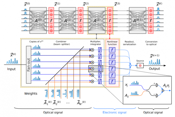 Image: / CC BY
The new AI accelerator architecture requires only one input and one output channel for each neuron. As a result, the number of photodetectors is equal to the number of neurons, rather than their weight coefficients.
This approach saves space on the chip, increases the number of useful signal pathways, and optimizes energy consumption. Currently, engineers from MIT are creating a prototype that will allow testing the capabilities of the new architecture in practice.
Who else is developing photonic chips
Developments of similar technology Lightelligence is a small startup based in Boston. Company employees say that their AI accelerator will enable machine learning tasks to be solved hundreds of times faster than traditional devices. Last year, the team was finishing the prototype of their device and preparing for testing.
Works in the field of photonic chips, as does Cisco. Earlier this year, the company announced the of the startup Luxtera, which designs photonic chips for data centers. In particular, the company produces hardware interfaces that enable fiber optics to be connected directly to servers. This approach increases network bandwidth and speeds up data transmission. Luxtera's devices use special lasers to encode information and germanium photodetectors to decode it.
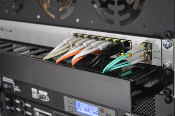
Photo - - Unsplash
Other major IT companies, such as Intel, are also engaged in optical technologies. Back in 2016, they began producing their own optical chips to optimize data transmission between data centers. Recently, representatives of the organization announced that they plan to implement these technologies beyond data centers — in lidar systems for autonomous vehicles.
What we have in the end
So far, photonic technologies cannot be called a universal solution. Their implementation requires significant investments in the technical re-equipment of data centers. However, developments like those being advanced at MIT and other organizations will make optical chips cheaper and likely allow them to be "pushed" into the mass market for data center equipment.
We at We help companies develop their IT infrastructure and provide private and hybrid cloud services. Here’s what we write about in our corporate blog:
Source: habr.com
