


For many years, scientists from around the world have been focused on two things — inventing and improving. At times, it is unclear which is more challenging. Take, for example, ordinary LEDs, which seem so simple and mundane that we hardly pay them any attention. However, if we add some excitons, a pinch of polaritons, and tungsten disulfide for flavor, these LEDs become anything but ordinary. All these intricate terms refer to highly unusual components that have enabled researchers from the City College of New York to create a new system capable of transmitting information very quickly using light. This development will enhance Li-Fi technology. What specific ingredients were used in this new technology, what is the recipe for this "dish," and how efficient is the new exciton-polariton LED? The report from the scientists will tell us. Let's go.
The foundation of the research
To simplify it to one word, this technology is light and everything associated with it. First, there are polaritons, which arise from the interaction of photons with excitations in the medium (phonons, excitons, plasmons, magnons, etc.). Secondly, excitons — electronic excitations in a dielectric, semiconductor, or metal, migrating through the crystal and not associated with the transfer of electric charge or mass.
It is important to note that these quasiparticles love cold; that is, their activity can only be observed at extremely low temperatures, which significantly limits their practical applications. But that was in the past. In this work, the scientists managed to overcome the temperature limitation and utilize them at room temperature.
The key feature of polaritons is their ability to bind photons together. Photons colliding with rubidium atoms acquire mass. In the process of multiple collisions, photons bounce off each other, but in rare cases, they form pairs and triplets, losing the atomic component represented by the rubidium atom.
However, to do something with light, it needs to be captured. For this purpose, an optical resonator is required, which consists of reflective elements that form a standing light wave.
In this research, even more unusual quasi-particles play a crucial role — exciton-polaritons, which are formed due to the strong coupling of excitons and photons captured in the optical resonator.
However, this is not enough, as a material basis is also necessary. And who better than the transition metal dichalcogenides (TMDs) to fulfill this role? More specifically, a monolayer of WS2 (tungsten disulfide) was used as the emitting material, which possesses impressive exciton binding energies, becoming one of the main criteria for selecting the material basis.
The combination of all the above elements has allowed for the creation of an electrically controlled polariton light-emitting diode operating at room temperature.
To implement this device, the WS2 monolayer is positioned between thin hexagonal tunneling barriers made of boron nitride (hBN), with graphene layers serving as electrodes.
Research Results
WS2, being a transition metal dichalcogenide, is also an atomically thin van der Waals (vdW) material. This indicates its unique electrical, optical, mechanical, and thermal properties.
In combination with other vdW materials such as graphene (as a conductor) and hexagonal boron nitride (hBN, as an insulator), a wide range of electrically controlled semiconductor devices, including light-emitting diodes, can be realized. Such combinations of van der Waals materials and polaritons have been previously implemented, as researchers openly state. However, in earlier studies, the resulting systems were complex and imperfect, and did not reveal the full potential of each component.
One of the ideas inspired by its predecessors is the use of a two-dimensional material platform. In this case, devices can be implemented with atomically thin emission layers that can be integrated with other vdW materials serving as contacts (graphene) and tunnel barriers (hBN). Moreover, such two-dimensionality allows for the combination of polaritonic light-emitting diodes with vdW materials that possess unusual magnetic properties, strong superconductivity, and/or non-standard topological carriers. As a result of this integration, a completely new type of device can emerge, whose properties may be quite unusual. However, as scientists say, this is a topic for another study.
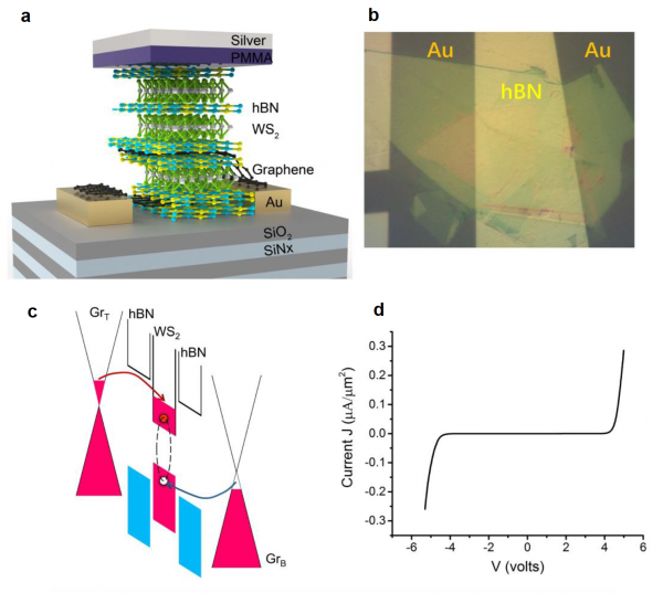
Image No. 1
In the image 1a a three-dimensional model of a device that resembles a layered cake is shown. The top mirror of the optical resonator is made of a silver layer, while the bottom one is a 12-layer distributed Bragg reflector*. The active area contains a tunnel region.
Distributed Bragg reflector* is a structure made of multiple layers in which the refractive index of the material changes periodically perpendicular to the layers.
The tunnel region consists of a vdW heterostructure made of a monolayer of WS2 (light-emitting layer), thin hBN layers on both sides of the monolayer (tunnel barrier), and graphene (transparent electrodes for injecting electrons and holes).
Two additional layers of WS2 were added to increase the overall strength of the generator and thus enhance the Rabi splitting of polariton states.
The mode of operation of the resonator is tuned by varying the thickness of the PMMA layer (polymethyl methacrylate, i.e., acrylic glass).
Image 1b is a photograph of the vdW heterostructure on the surface of the distributed Bragg reflector. Due to the high reflectivity of the distributed Bragg reflector serving as the bottom layer, the tunnel region in the photograph has a very low reflection contrast, resulting in only the upper thick layer of hBN being visible.
Chart 1c represents the vdW heterostructure diagram in tunnel geometry under bias. Electroluminescence (EL) is observed above the threshold voltage when the Fermi level of the upper (lower) graphene is shifted above (below) the conduction (valence) band of WS2, allowing an electron (hole) to tunnel into the conduction (valence) band of WS2. This creates favorable conditions for the formation of excitons in the WS2 layer with subsequent radiative (emissive) recombination of electron-hole pairs.
Unlike light emitters based on p-n junctions, which require doping to function, the EL from tunneling devices depends solely on the tunneling current, allowing to avoid optical losses and any changes in resistivity caused by temperature variations. At the same time, the tunneling architecture permits a much larger emission area compared to p-n junction-based dichalcogenide devices.
Image 1d demonstrates the electric characteristics of tunneling current density (J) as a function of bias voltage (V) between graphene electrodes. The sharp increase in current for both positive and negative voltages indicates the emergence of tunneling current through the structure. With an optimal hBN layer thickness (~2 nm), a significant tunneling current and increased lifetime of injected carriers for radiative recombination are observed.
Before conducting the electroluminescent experiment, characterization of the device was performed using white light reflectivity with angular resolution to confirm the presence of strong exciton coupling.
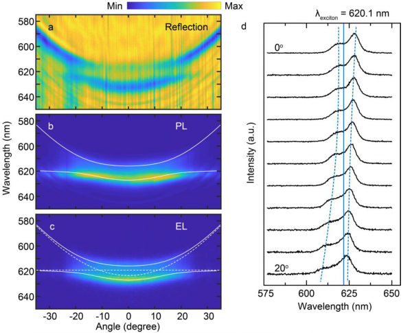
Image #2
In the image 2a shows reflection spectra with angular resolution from the active area of the device, demonstrating behavior that hinders crossing. Photoluminescence (PL) was also observed under non-resonant excitation (460 nm), demonstrating intense emission from the lower branch of the polariton and weaker emission from the upper branch of the polariton (2b).
At 2c the dispersion of electroluminescence of the polariton is shown at an injection of 0.1 μA/mk². The Rabi splitting and the resonator detuning, obtained by fitting the oscillator modes (solid and dashed white lines) to the electroluminescent experiment, are approximately 33 meV and -13 meV, respectively. The resonator detuning is defined as δ = Ec − Ex, where Ex is the exciton energy, and Ec is the energy of the resonator photon with zero momentum in the plane. The graph 2d this is a cut at different angles from the electroluminescent dispersion. Here, the dispersion of the upper and lower polariton modes is clearly visible, with an anti-crossing occurring in the exciton resonance region.
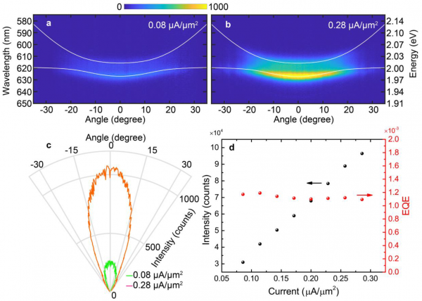
Image #3
As the tunneling current increases, the total intensity of the EL increases. Weak EL from polaritons is observed near the threshold shift (3a), while at sufficiently high shifts above the threshold, the polariton emission becomes distinct (3b).
In the image 3c a polar plot of the EL intensity is shown as a function of angle, depicting a narrow emission cone of ± 15°. The radiation pattern remains virtually unchanged for both the minimum (green curve) and maximum (orange curve) excitation currents. At 3d the integrated intensity at various flowing tunneling currents is shown, which, as seen from the graph, is quite linear. Thus, increasing the current to high values can lead to successful scattering of polaritons along the lower branch and create an extremely narrow radiation pattern due to polariton generation. However, in this experiment, it was not possible to achieve this due to the limitation associated with the dielectric breakdown of the tunneling barrier hBN.
The red dots on 3d show measurements of another parameter — the external quantum efficiency*.
Quantum efficiency* is the ratio of the number of photons whose absorption led to the formation of quasiparticles to the total number of absorbed photons.
The observed quantum efficiency is comparable to that of other polaritonic light-emitting diodes (based on organic materials, carbon nanotubes, etc.). It is worth noting that in the studied device, the thickness of the light-emitting layer is only 0.7 nm, whereas for other devices this value is significantly higher. The researchers acknowledge that the quantum efficiency of their device is not the highest, but it can be improved by placing more monolayers within the tunneling zone, separated by thin hBN layers.
The researchers also investigated the influence of the resonator disorder on the polariton EL by fabricating another device with a stronger disorder (-43 meV).
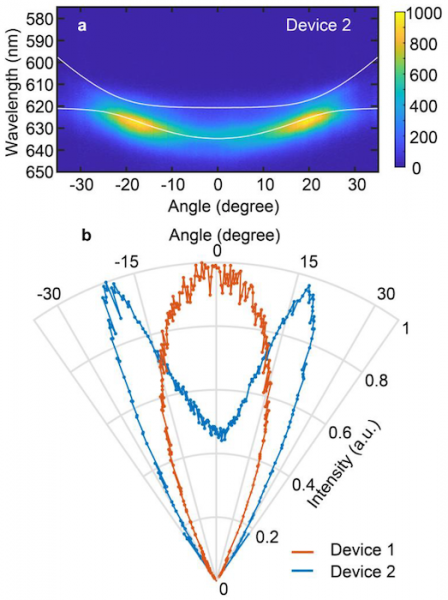
Image No. 4
In the image 4a The spectra of the EL with angular resolution of this device are shown at a current density of 0.2 µA/m². Due to strong disorder, the device demonstrates a pronounced bottleneck effect in the EL with the emission maximum occurring at a large angle. This is further confirmed in the image. 4b, where the polar plots of this device are compared with the first (2c).
For a more detailed understanding of the nuances of the research, I recommend checking out the .
Epilogue
Thus, all the observations and measurements described above confirm the presence of polaritonic electroluminescence in the vdW heterostructure embedded in an optical microresonator. The tunneling architecture of the studied device facilitates the injection of electrons/holes and recombination in the WS2 monolayer, which serves as the light emitter. Importantly, the tunneling mechanism of the device does not require doping of the components, minimizing losses and various temperature-related changes.
It has been established that the EL is highly directional due to the resonator dispersion. Consequently, improving the quality factor of the resonator and higher current input will enhance the efficiency of microresonator light-emitting diodes, as well as electrically driven microresonator polaritons and photonic lasers.
This work once again confirmed that transition metal dichalcogenides possess truly unique properties and a wide range of applications.
Such research and innovative inventions can significantly impact the development and dissemination of data transmission technologies through LEDs and light itself. Futuristic technologies like Li-Fi can provide much greater speeds than the currently available Wi-Fi.
Thank you for your attention, stay curious, and have a great working week, everyone! 🙂
Thank you for staying with us. Do you enjoy our articles? Would you like to see more interesting materials? Support us by placing an order or recommending us to your friends. 30% discount for Habr users on a unique entry-level server designed by us for you: (options available with RAID1 and RAID10, up to 24 cores and up to 40GB DDR4).
Dell R730xd for half the price? Only with us in the Netherlands! Dell R420 — 2x E5-2430 2.2GHz 6C 128GB DDR3 2x960GB SSD 1Gbps 100TB — from $99! Read about how
Source: habr.com
