

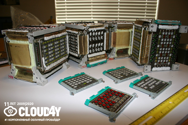
The Launch Vehicle Digital Computer (LVDC) played a key role in the Apollo lunar program, driving the Saturn 5 rocket. Like most computers of the time, it stored data in tiny magnetic cores. In this article, Cloud4Y talks about the LVDC memory module from the deluxe Steve Jurvetson.
This memory module was improved in the mid-1960s. It was built using surface-mount components, hybrid modules, and flexible connections, making it an order of magnitude smaller and lighter than conventional computer memory of the time. However, the memory module allowed to store only 4096 words of 26 bits.
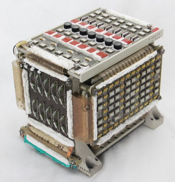
Magnetic core memory module. This module stores 4K words of 26 data bits and 2 parity bits. With four memory modules giving a total capacity of 16 words, it weighs 384 kg and measures 2,3 cm × 14 cm × 14 cm.
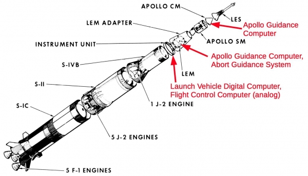
The moon landing began on May 25, 1961, when President Kennedy announced that America would put a man on the moon before the end of the decade. For this, a three-stage Saturn 5 rocket was used, the most powerful rocket ever created. Saturn 5 was controlled and controlled by a computer (here about him) the third stage of a launch vehicle, starting from takeoff into Earth's orbit, and then on its way to the Moon. (The Apollo spacecraft was separating from the Saturn V rocket at this point, and the LVDC mission was completed.)
The LVDC is installed in the base frame. Circular connectors are visible on the front of the computer. Used 8 electrical connectors and two connectors for liquid cooling
The LVDC was just one of several computers aboard the Apollo. The LVDC was connected to the flight control system, a 45 kg analog computer. The onboard Apollo Guidance Computer (AGC) guided the spacecraft to the lunar surface. The command module contained one AGC while the lunar module contained a second AGC along with the Abort navigation system, a spare emergency computer.
There were several computers on board the Apollo.
Unit Logic Devices (ULD)
LVDC was created using an interesting hybrid technology called ULD, unit load device. Although they looked like integrated circuits, ULD modules contained several components. They used simple silicon chips, each with only one transistor or two diodes. These arrays, along with printed thick-film printed resistors, were mounted on a ceramic wafer to implement circuits such as a logic gate. These modules were a variant of the SLT modules () designed for the popular IBM S/360 series computers. IBM began developing SLT modules in 1961, before integrated circuits were commercially viable, and by 1966, IBM was producing over 100 million SLT modules a year.
The ULD modules were significantly smaller than the SLT modules, as seen in the photo below, making them more suitable for a compact space computer. The ULD modules used ceramic pads instead of the metal pins in the SLT, and had metal contacts on the top surface instead of pins. Clips on the board held the ULD module in place and connected to these pins.
Why did IBM use SLT modules instead of integrated circuits? The main reason was that integrated circuits were still in their infancy, having been invented in 1959. In 1963, SLT modules had cost and performance advantages over integrated circuits. However, SLT modules were often viewed as inferior to integrated circuits. One of the advantages of SLT modules over integrated circuits was that the resistors in SLTs were much more accurate than those in integrated circuits. During manufacture, the thick film resistors in the SLT modules were carefully sandblasted to remove the resistive film until they achieved the desired resistance. SLT modules were also cheaper than comparable integrated circuits in the 1960s.
The LVDC and related equipment used over 50 different types of ULDs.
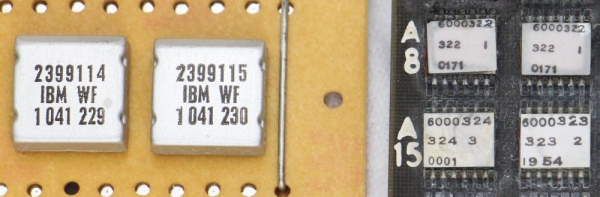
SLT modules (left) are significantly larger than ULD modules (right). ULD size is 7,6mm×8mm
The photo below shows the internal components of the ULD module. On the left side of the ceramic plate are conductors connected to four tiny square silicon crystals. It looks like a circuit board, but keep in mind that it is much smaller than a fingernail. The black rectangles on the right are thick film resistors printed on the underside of the plate.
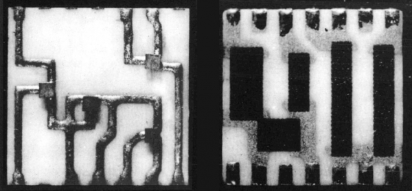
ULD, top and bottom view. Silicon crystals and resistors are visible. While SLT modules had resistors on the top surface, ULD modules had resistors on the bottom, which increased density as well as cost.
The photo below shows a silicon die from the ULD module, which implemented two diodes. The sizes are unusually small, for comparison, there are sugar crystals nearby. The crystal had three external connections through copper balls soldered to three circles. The bottom two circles (the anodes of the two diodes) were doped (darker areas), while the top right circle was the cathode connected to the base.
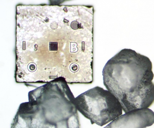
Photograph of a two-diode silicon crystal next to sugar crystals
How magnetic core memory works
Magnetic core memory was the main form of data storage in computers from the 1950s until it was replaced by solid state storage devices in the 1970s. Memory was created from tiny ferrite rings called cores. Ferrite rings were placed in a rectangular matrix and two to four wires passed through each ring to read and write information. The rings allowed one bit of information to be stored. The core was magnetized using a current pulse through the wires passing through the ferrite ring. The direction of magnetization of one core could be changed by sending a pulse in the opposite direction.
To read the value of the core, a current pulse put the ring in state 0. If the core had previously been in state 1, the changing magnetic field created a voltage in one of the wires running through the cores. But if the core were already in state 0, the magnetic field would not change and the sense wire would not rise in voltage. So the value of the bit in the core was read by resetting it to zero and checking the voltage on the read wire. An important feature of memory on magnetic cores was that the process of reading a ferrite ring destroyed its value, so the core had to be "rewritten".
It was inconvenient to use a separate wire to change the magnetization of each core, but in the 1950s, a ferrite memory was developed that worked on the principle of coincidence of currents. The four-wire circuit—X, Y, Sense, Inhibit—has become commonplace. The technology exploited a special property of cores called hysteresis: a small current does not affect the ferrite memory, but a current above a threshold would magnetize the core. When energized with half the required current on one X line and one Y line, only the core in which both lines crossed received enough current to remagnetize, while the other cores remained intact.
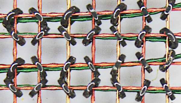
This is what the memory of the IBM 360 Model 50 looked like. The LVDC and the Model 50 used the same type of core, known as 19-32 because their inner diameter was 19 mils (0.4826 mm) and their outer diameter was 32 mils (0,8 mm). You can see in this photo that there are three wires running through each core, but LVDC used four wires.
The photo below shows one rectangular LVDC memory array. 8 This matrix has 128 X-wires running vertically and 64 Y-wires running horizontally, with a core at each intersection. A single read wire runs through all cores parallel to the Y-wires. The write wire and the inhibit wire run through all cores parallel to the X wires. The wires cross in the middle of the matrix; this reduces the induced noise because the noise from one half cancels out the noise from the other half.
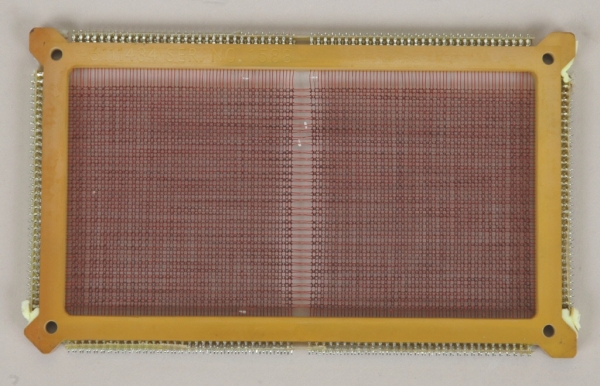
One LVDC ferrite memory matrix containing 8192 bits. Connection with other matrices is carried out through pins on the outside
The matrix above had 8192 elements, each storing one bit. To save a memory word, several basic matrices were added together, one for each bit in the word. Wires X and Y snaked through all the main matrices. Each matrix had a separate read line and a separate write inhibit line. LVDC memory used a stack of 14 base matrices (below) storing a 13-bit "syllable" along with a parity bit.
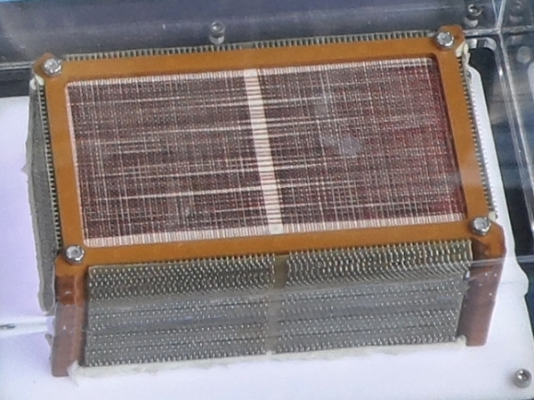
The LVDC stack consists of 14 main matrices
Writing to magnetic core memory required additional wires, the so-called inhibition lines. Each matrix had one inhibition line running through all the cores in it. During the write process, current passes through the X and Y lines, remagnetizing the selected rings (one per plane) to state 1, keeping all 1s in the word. To write a 0 at the bit position, the line was energized with half the current opposite to the X line. As a result, the cores remained at 0. Thus, the inhibit line did not allow the core to flip to 1. Any desired word could be written to memory by activating the corresponding inhibit lines.
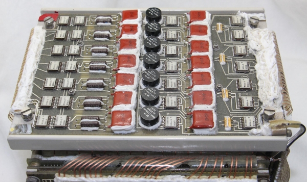
LVDC memory module
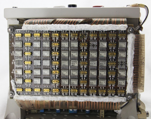
How is an LVDC memory module physically constructed? In the center of the memory module is a stack of 14 ferromagnetic memory arrays shown earlier. It is surrounded by several boards with circuitry to drive the X and Y wires and the inhibit lines, bit read lines, error detection, and generating the necessary clock signals.
In general, most of the memory-related circuitry is in the LVDC computer logic, not in the memory module itself. In particular, computer logic contains registers for storing addresses and data words and converting between serial and parallel. It also contains circuitry for reading from the read bit lines, error checking, and clocking.
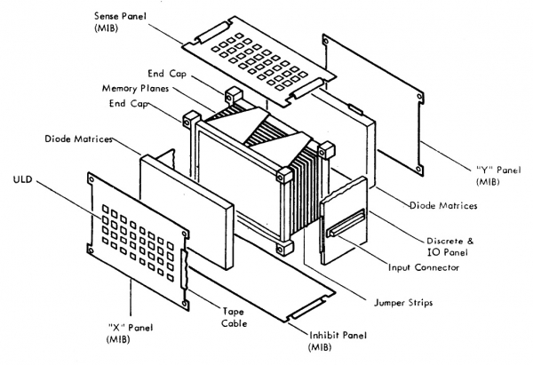
Memory module showing key components. MIB (Multilayer Interconnection Board) is a 12-layer printed circuit board
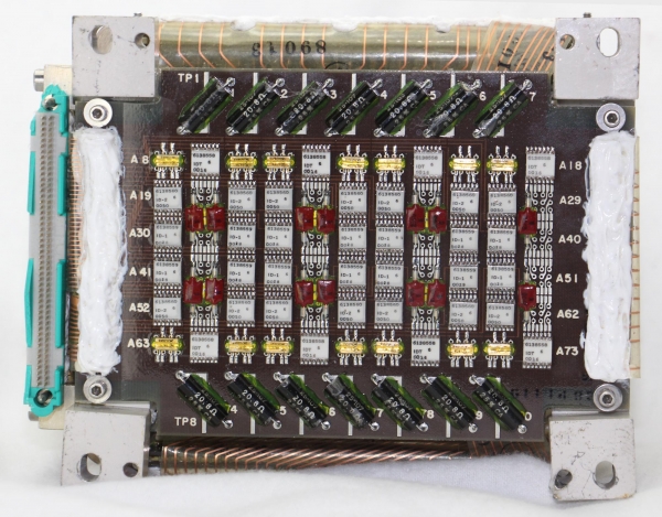
Y memory driver board
A word in core memory is selected by passing the respective X and Y lines through the main board stack. Let's start by describing the Y-driver circuit and how it generates a signal through one of the 64 Y-lines. Instead of 64 separate driver circuits, the module reduces the number of circuits by using 8 "high" drivers and 8 "low" drivers. They are wired in a "matrix" configuration, so each combination of high and low drivers selects different rows. Thus, 8 "high" and 8 "low" drivers select one of the 64 (8 × 8) Y-lines.
Y driver board (front) drives the Y select lines in the stack of boards
In the photo below you can see some of the ULD modules (white) and the pair of transistors (gold) that drive the Y select lines. The "EI" module is the heart of the driver: it supplies a constant voltage pulse (E) or passes a constant current pulse (I) through the selection line. The select line is controlled by activating the EI module in voltage mode at one end of the line and the EI module in current mode at the other end. The result is a pulse with the correct voltage and current, sufficient to remagnetize the core. It takes a lot of momentum to turn it over; the voltage pulse is fixed at 17 volts, and the current ranges from 180 mA to 260 mA depending on the temperature.
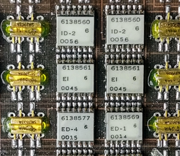
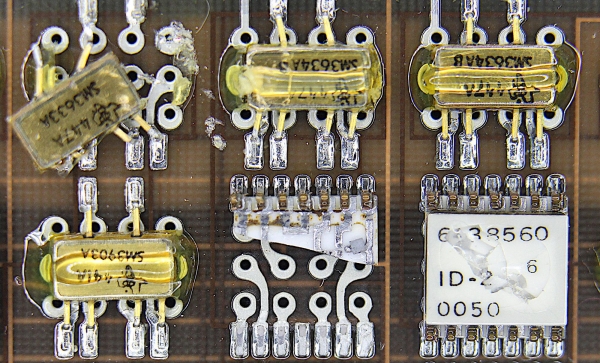
Macro photo of the Y driver board showing six ULD modules and six pairs of transistors. Each ULD module is labeled with an IBM part number, module type (for example, "EI"), and a code whose meaning is unknown
The board is also equipped with error monitor (ED) modules that detect when more than one Y select line is activated at the same time. The ED module uses a simple semi-analogue solution: it sums the input voltages using a network of resistors. If the resulting voltage is above the threshold, the key is triggered.
Under the driver board is a diode array containing 256 diodes and 64 resistors. This matrix converts the 8 top and 8 bottom pairs of signals from the driver board into 64 Y-line connections that run through the main stack of boards. Flexible cables at the top and bottom of the board connect the board to the diode array. Two flex cables on the left (not visible in the photo) and two busbars on the right (one visible) connect the diode matrix to the array of cores. The flex cable visible on the left connects the Y-board to the rest of the computer via the I/O board, while the small flex cable on the bottom right connects to the clock generator board.
X Memory Driver Board
The layout for driving the X lines is the same as the Y scheme, except there are 128 X lines and 64 Y lines. Because there are twice as many X wires, the module has a second X driver board underneath it. Although the X and Y boards have the same components, the wiring is different.
This board and the one below it control X selected rows in a stack of core boards
The photo below shows that some components were damaged on the board. One of the transistors is displaced, the ULD module is broken in half, and the other is broken off. The wiring is visible on the broken module, along with one of the tiny silicon crystals (right). In this photo, you can also see the traces of vertical and horizontal conductive tracks on a 12-layer printed circuit board.
Close-up of the damaged section of the board
Below the X driver boards is an X diode matrix containing 288 diodes and 128 resistors. The X-diode array uses a different topology than the Y-diode board to avoid doubling the number of components. Like the Y-diode board, this board contains components mounted vertically between two printed circuit boards. This method is called "cordwood" and allows the components to be tightly packed.
A macro photo of an X diode array showing vertically mounted cordwood diodes between 2 printed circuit boards. The two X driver boards sit above the diode board, separated from them by polyurethane foam. Please note that the printed circuit boards are very close to each other.
Memory Amplifiers
The photo below shows the readout amplifier board. Has 7 channels for reading 7 bits from the memory stack; the identical board below handles 7 more bits for a total of 14 bits. The purpose of the sense amplifier is to detect the small signal (20 millivolts) generated by the remagnetizable core and turn it into a 1-bit output. Each channel consists of a differential amplifier and buffer, followed by a differential transformer and output clamp. On the left, a 28-wire flex cable connects to the memory stack, leading the two ends of each sense wire to an amplifier circuit, starting with the MSA-1 (Memory Sense Amplifier) module. The individual components are resistors (brown cylinders), capacitors (red), transformers (black), and transistors (gold). The data bits exit the sense amplifier boards via the flexible cable on the right.
Readout amplifier board at the top of the memory module. This board amplifies the signals from the sense wires to create output bits
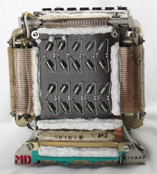
Write Inhibit Line Driver
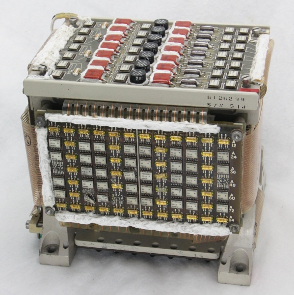
Inhibit drivers are used to write to memory and are located on the underside of the main module. There are 14 inhibit lines, one for each matrix on the stack. To write a 0 bit, the corresponding lock driver is activated and the current through the inhibit line prevents the core from switching to 1. Each line is driven by an ID-1 and ID-2 module (write inhibit line driver) and a pair of transistors. Precision 20,8 ohm resistors at the top and bottom of the board regulate the blocking current. The 14-wire flex cable on the right connects the drivers to the 14 inhibit wires in the stack of core boards.
Inhibition board at the bottom of the memory module. This board generates 14 inhibit signals used during recording
Clock driver memory
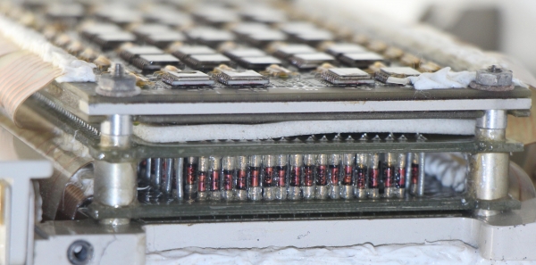
The clock driver is a pair of boards that generate clock signals for the memory module. Once the computer begins a memory operation, the various clock signals used by the memory module are generated asynchronously by the module's clock driver. The clock drive boards are located at the bottom of the module, between the stack and the inhibit board, so the boards are hard to see.
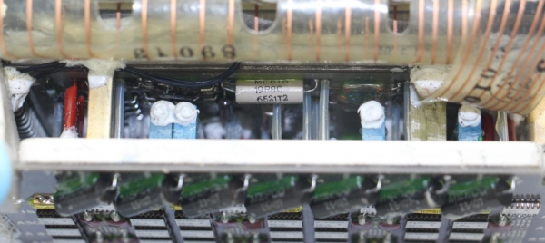
The clock driver boards are below the main memory stack but above the lock board
The blue board components in the photo above are multi-turn potentiometers, presumably for timing or voltage adjustment. Resistors and capacitors are also visible on the boards. The diagram shows several MCD (Memory Clock Driver) modules, but no modules are visible on the boards. It's hard to tell if this is due to limited visibility, a circuit change, or the presence of another board with these modules.
Memory I/O Panel
The last memory module board is the I/O board, which distributes signals between the memory module boards and the rest of the LVDC computer. The green 98-pin connector at the bottom connects to the LVDC memory chassis, providing signals and power from the computer. Most of the plastic connectors are broken, which is why the contacts are visible. The distribution board is connected to this connector by two 49-pin flexible cables at the bottom (only the front cable is visible). Other flex cables distribute signals to the X Driver Board (left), Y Driver Board (right), Sense Amplifier Board (top), and Inhibit Board (bottom). 20 capacitors on the board filter the power supplied to the memory module.
The I/O board between the memory module and the rest of the computer. The green connector at the bottom connects to the computer and these signals are routed through flat cables to other parts of the memory module
Final World
The main LVDC memory module provided compact, reliable storage. Up to 8 memory modules could be placed in the bottom half of the computer. This allowed the computer to store 32 26-bit words or 16 kilowords in redundant highly reliable "duplex" mode.
One interesting feature of LVDC was that memory modules could be mirrored for reliability. In "duplex" mode, each word was stored in two memory modules. If an error occurred in one module, the correct word could be obtained from another module. While this provided reliability, it cut the memory footprint in half. Alternatively, the memory modules can be used in "simplex" mode, with each word stored once.
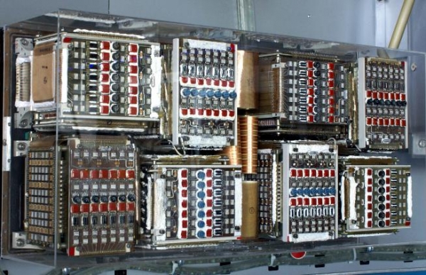
LVDC accommodated up to eight CPU memory modules
The magnetic core memory module provides a visual representation of the time when 8 KB storage required a 5-pound (2,3 kg) module. However, this memory was very perfect for its time. Such devices fell into disuse in the 1970s with the advent of semiconductor DRAMs.
The contents of RAM are preserved when the power is turned off, so it is likely that the module is still storing software from the last time the computer was used. Yes, yes, there you can find something interesting even decades later. It would be interesting to try to recover this data, but the damaged circuitry creates a problem, so the contents will probably not be able to be retrieved from the memory module for another decade.
What else can you read on the blog?
→
→
→
→
→
Subscribe to our -channel, so as not to miss the next article! We write no more than twice a week and only on business. We also remind you that Cloud4Y can provide secure and reliable remote access to business applications and information necessary for business continuity. Remote work is an additional barrier to the spread of coronavirus. Details are from our managers.
Source: habr.com
