

I am demonstrating the simplest way to recover data from the NAND memory of a smartphone, regardless of the reason you need to do this. In some cases, the phone is inoperable due to a damaged processor, or the motherboard is washed and beyond recovery; in other cases, the phone is locked, and data needs to be saved.
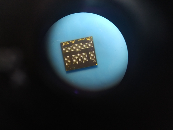
I was fortunate to work at fix-oscomp, a division of the OSKOMP company that repairs digital equipment. This is where I became practically familiar with this method.
NAND is a type of flash memory most commonly used in modern smartphones.
NAND structure according to Wikipedia
The NAND structure is a three-dimensional array. It is based on the same matrix as NOR, but instead of one transistor at each intersection, a column of series-connected cells is installed. This arrangement results in many gate lines at one intersection. The density of the layout can be significantly increased (since only one gate conductor connects to each cell in the column), but the access algorithm for reading and writing cells becomes noticeably more complex. Additionally, there are two MOS transistors installed in each line. A control transistor for the discharge line (bit line select transistor), located between the column of cells and the discharge line. And a ground select transistor located before ground.
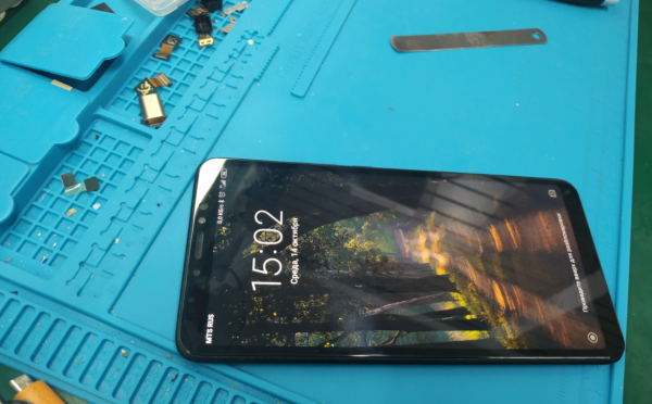
Today's patient is the Xiaomi Mi Max 3:
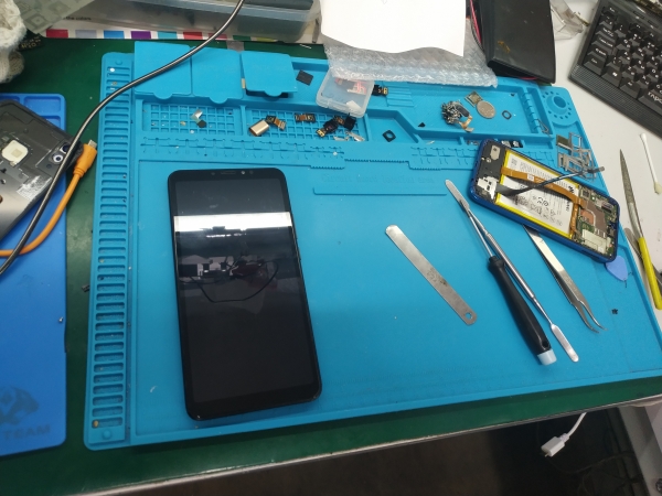
After being submerged, it stopped turning on.
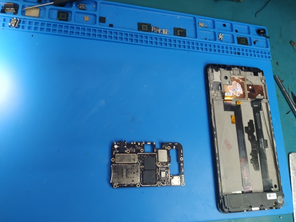
Diagnosis showed that the processor is more dead than alive. The client needs data from the phone and possible recovery of the device itself.
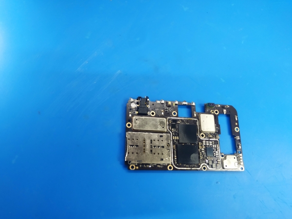
The board was cleaned, but we cannot replace the processor, as the processor and NAND memory are paired by a key, and we change them in pairs as well. In this case, we take the donor board from a cheaper model; in this case, the Xiaomi Redmi Note 5 will do.
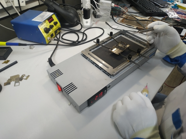
We heat the board with bottom heating.
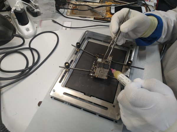
We apply flux.
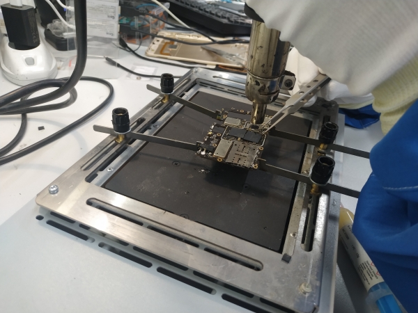
We heat up with a heat gun.
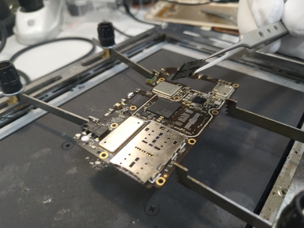
We remove the NAND memory.
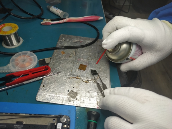
We clean off the residue of flux.
We check the contacts.
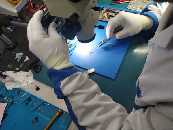
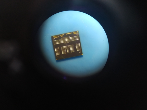
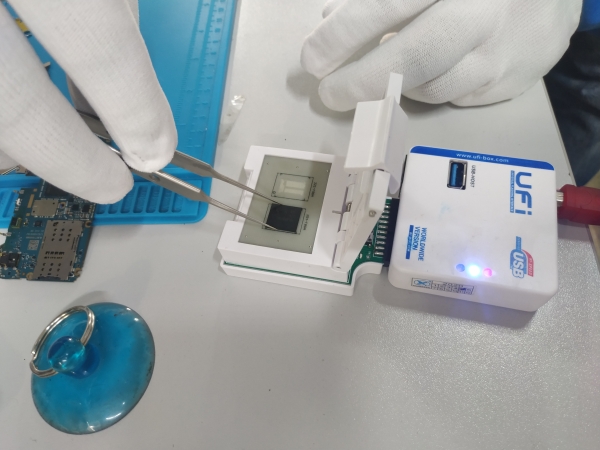
We install the memory in the reading device.
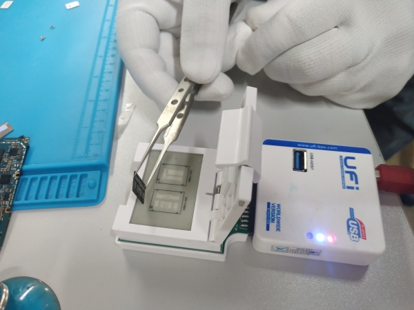
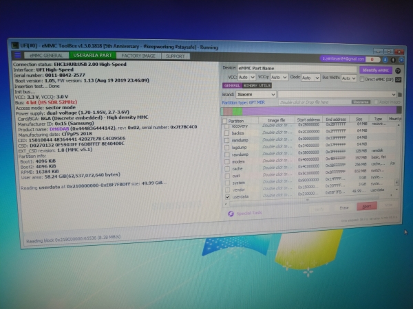
In our case, we need the userdata and boot files.
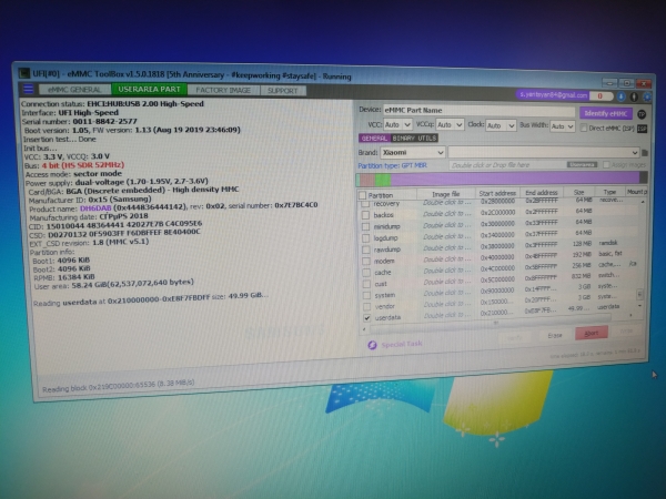
Speed up to 10 MiB/s. But you will have to wait a long time. The reading process takes an average of 2 hours.
This way, we can increase the volume of memory and RAM if necessary.
We write the data onto the donor memory.
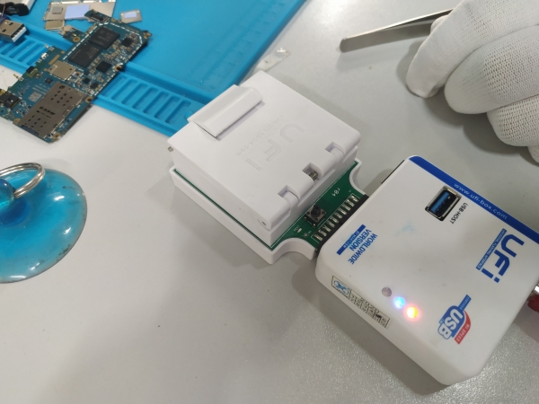
We solder the memory and processor from the donor, turn it on, and enjoy!
Thank you for your attention!
Source: habr.com
