

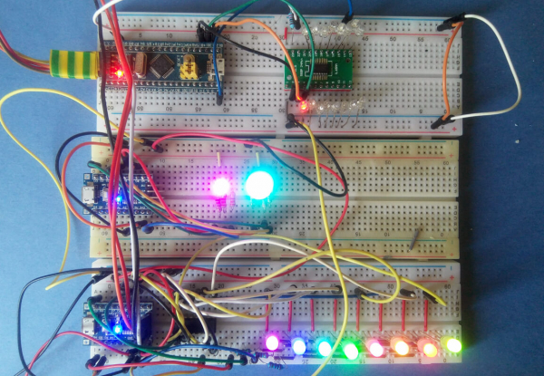
In I tried to explain to hobbyist electronics enthusiasts, who have outgrown their Arduino phase, how and why they should read datasheets and other documentation for microcontrollers. The text turned out to be lengthy, so I promised to provide practical examples in a separate article. Well, here I am.
Today, I will show how to solve fairly simple yet essential tasks for numerous projects using datasheets with STM32 (Blue Pill) and STM8 controllers. All demo projects will focus on my favorite LEDs, which we will light up in large quantities, requiring the involvement of various interesting peripherals.
The text again turned out to be huge, so for convenience, I am providing a table of contents:
Disclaimer: I am not an engineer and do not claim to have deep knowledge in electronics; this article is meant for enthusiasts like me. In fact, I considered myself two years ago as the target audience. If someone had told me back then that reading datasheets for an unfamiliar chip is not scary, I wouldn't have wasted so much time searching for code snippets online and creating makeshift solutions with scissors and adhesive tape.
The focus of this article is on datasheets, not projects, so the code may not be overly polished and often cobbled together. The projects themselves are very simple, yet suitable for a first encounter with a new chip.
I hope my article helps someone who is at a similar stage of immersing themselves in the hobby.
STM32
16 LEDs with DM634 and SPI
A small project using the Blue Pill (STM32F103C8T6) and the DM634 LED driver. We will explore the driver, STM I/O ports, and set up SPI using datasheets.
DM634
A Taiwanese chip with 16 16-bit PWM outputs, which can be connected in chains. The lower 12-bit model is known from a domestic project. At one time, while choosing between the DM63x and the well-known TLC5940, I settled on the DM for several reasons: 1) the TLC on AliExpress is definitely counterfeit, while this one is not; 2) the DM has its own PWM with a frequency generator; 3) it could be bought cheaply in Moscow instead of waiting for a package from Ali. And of course, I was curious to learn how to control the chip myself rather than using a ready-made library. Currently, chips are mainly available in SSOP24 packages, which are easy to solder onto an adapter.
Since the manufacturer is Taiwanese, for the chip is written in Chinglish, so it will be fun. First, we look at the pinout (Pin Connection), to understand which pin connects to what, and the description of the pins (Pin Description). 16 outputs:

Incoming constant current sources (open drain)
Sink / Open-drain output – drain; current sink; output, when active connected to ground, – the anodes of the LEDs are connected to the driver. Electrically, this is, of course, not an 'open drain' (open drain), but this designation for pins in drain mode is often found in datasheets.

External resistors between REXT and GND to set the output current value
A reference resistor is placed between the REXT pin and ground, controlling the internal resistance of the outputs, see the graph on page 9 of the datasheet. In the DM634, this resistance can also be controlled programmatically by setting the overall brightness (global brightness); I won't go into details in this article, I'll just place a resistor of 2.2 – 3 kOhm here.
To understand how to control the chip, let's look at the device interface description:
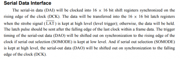
Aha, here it is, Chinglish at its finest. Translating this is tricky, it can be understood with some effort, but there’s another way – let’s take a look at how the connection is described in the datasheet for the functionally similar TLC5940:

… Only three pins are required to input data into the device. The rising edge of the SCLK signal shifts data from the SIN pin into the internal register. After all the data has been loaded, a short high signal on XLAT sequentially latches the transmitted data into the internal registers. The internal registers are edge-triggered latches activated by the level of the XLAT signal. All data is transmitted MSB first.
Latch – latch/lock.
Rising edge – front edge of the pulse
MSB first – with the most significant (leftmost) bit forwarded.
to clock data – to transmit data sequentially (bit by bit).
The term latch is often found in chip documentation and is translated in various ways, so for clarity, I will allow myself a
brief primerAn LED driver essentially functions as a shift register. The term "shift" (shift) in its name refers to the bitwise movement of data within the device: each newly inserted bit pushes the entire chain forward. Since no one wants to witness chaotic blinking of the LEDs during shifting, the process occurs in buffer registers, separated from the working area by a gate (latch) – this serves as a sort of anteroom where bits are arranged in the necessary sequence. Once everything is ready, the gate opens, and the bits go to work, replacing the previous batch. The term latch in microchip documentation almost always implies such a gate, regardless of the combinations in which it is used.
Thus, data transmission in the DM634 is carried out as follows: set the DAI input to the value of the most significant bit of the distant LED, pull DCK up and down; set the DAI input to the value of the next bit, pull DCK; and so forth until all bits are transmitted (clocked in), after which pull LAT. This can be done manually (bit-bang), but it's better to use a specialized SPI interface designed for this purpose, which is available on our STM32 in two instances.
Blue Pill STM32F103
Overview: STM32 controllers are significantly more complex than Atmega328 might suggest. At startup, for power-saving reasons, almost all peripherals are disabled, and the clock frequency is set to 8 MHz from an internal source. Fortunately, STM programmers have written code that brings the chip up to a "calculated" 72 MHz, and the authors of all IDEs I know have included it in the initialization procedure, so we don't need to clock it (but ). However, you'll need to enable the peripherals.
Documentation: The Blue Pill features the popular STM32F103C8T6 chip, for which there are two useful documents:
- for STM32F103x8 and STM32F103xB microcontrollers;
- for the entire STM32F103 line and beyond.
In the datasheet, we may be interested in:
- Pinouts – pin configurations of the chips – in case we decide to make our own boards;
- Memory Map – a memory map for a specific chip. The Reference Manual contains a map for the entire lineup, which mentions registers that we don't have.
- Pin Definitions Table – a list of main and alternative pin functions; for the 'Blue Pill,' you can find more convenient images with a list of pins and their functions on the internet. So, let's immediately Google Blue Pill pinout and keep an image like this handy:
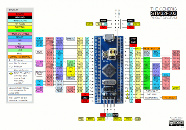
NB: the image from the internet had an error noted in the comments, for which thanks. The image has been replaced, but this is a lesson – it's better to verify information not from datasheets.
We remove the datasheet, open the Reference Manual, and from now on we'll use only it.
Procedure: we deal with standard input/output, configure SPI, and enable the necessary peripherals.
Input/Output
On the Atmega328, input/output is implemented very simply, which can confuse due to the abundance of options in STM32. Right now, we need only outputs, but even they have four variants:

open-drain output, push-pull output, alternate push-pull, alternate open-drain
Push-pull (push-pull) – the familiar output from Arduino, the pin can take either a HIGH or LOW value. However, with open-drain, there are , although in reality, it’s all quite simple:
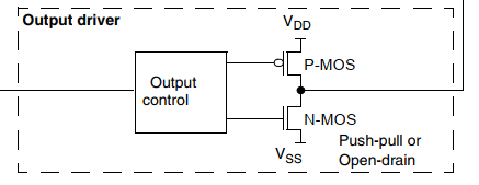
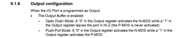
Output configuration / when the port is assigned to output: / output buffer enabled: / – open-drain mode: '0' in the output register activates N-MOS, '1' in the output register keeps the port in Hi-Z mode (P-MOS is not activated) / – push-pull mode: '0' in the output register activates N-MOS, '1' in the output register activates P-MOS.
The only difference between open-drain (open drain) and push-pull (push-pull) is that in the former, the pin cannot take a HIGH state: when writing a one to the output register, it switches to high impedance mode (high impedance, Hi-Z). When writing a zero, the pin behaves the same in both modes, both logically and electrically.
In normal output mode, the pin simply transmits the content of the output register. In 'alternative' mode, it is controlled by the corresponding peripheral (see 9.1.4):

If a port bit is configured as an alternative function output, the output register is disabled, and the pin is connected to the peripheral's output signal.
The alternative functionality of each pin is described in Pin Definitions The datasheet is available in the downloaded image. In response to the question of what to do if a pin has multiple alternative functions, the note in the datasheet provides guidance:

If multiple peripheral blocks use the same pin, to avoid conflicts between alternative functions, only one peripheral block should be used at a time, switching using the peripheral activation bit in the appropriate RCC register.
Finally, output pins also have a clock speed. This is another power-saving feature; in our case, we simply set it to maximum and forget about it.
So: we are using SPI, which means two pins (with data and clock signal) should be the 'push-pull alternative function', while another one (LAT) should be a 'regular push-pull'. But before assigning them, let's sort out SPI.
SPI
Another little tutorial
SPI, or Serial Peripheral Interface, is a simple and quite efficient interface for connecting microcontrollers to other microcontrollers and the outside world. Its working principle has already been described above, where the Chinese LED driver was discussed (refer to section 25 in the reference manual). SPI can operate in master and slave modes. It has four basic channels, not all of which need to be used:
- MOSI, Master Output / Slave Input: this pin sends data in master mode and receives data in slave mode;
- MISO, Master Input / Slave Output: conversely, it receives data in master mode and sends data in slave mode;
- SCK, Serial Clock: sets the data transfer frequency in master mode or receives the clock signal in slave mode. Essentially, it ticks off the bits;
- SS, Slave Select: this channel lets the slave know that it is being requested for something. On STM32, it is called NSS, where N = negative, that is, the controller becomes a slave when this channel is grounded. It works well in combination with Open Drain Output mode, but that's another story.
Like everything else, SPI on STM32 is feature-rich, which somewhat complicates its understanding. For example, it can work not only in SPI mode but also in I2S mode, and in the documentation, their descriptions are intermingled, so one must carefully filter out the unnecessary. Our task is quite simple: we just need to transmit data utilizing only MOSI and SCK. Let's go to section 25.3.4 (half-duplex communication), where we find 1 clock and 1 unidirectional data wire (1 clock signal and 1 unidirectional data flow):
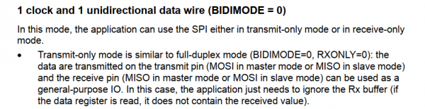
In this mode, the application uses SPI either in transmit-only or receive-only mode. The transmit-only mode is similar to the duplex mode: data is transmitted via the transmitting pin (MOSI in master mode or MISO in slave mode), and the receiving pin (MISO or MOSI respectively) can be used as a regular input/output pin. In this case, the application can simply ignore the Rx buffer (if read, it will not contain any transmitted data).
Great, the MISO pin is now free, let's connect the LAT signal to it. We'll figure out the Slave Select, which can be controlled programmatically on STM32, which is extraordinarily convenient. Let's read the corresponding paragraph in section 25.3.1 SPI General Description:

Software control of NSS (SSM = 1) / Slave selection information is contained in the SSI bit of the SPI_CR1 register. The external NSS pin remains available for other application needs.
It's time to write to the registers. I've decided to use SPI2, let's find its base address in the datasheet – in section 3.3 Memory Map:

Now let's begin:
#define _SPI2_(mem_offset) (*(volatile uint32_t *)(0x40003800 + (mem_offset)))Open section 25.3.3 with the telling title "Setting up SPI in master mode":
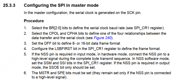
1. Set the clock frequency of the serial interface using the BR[2:0] bits in the SPI_CR1 register.
The registers are gathered in the corresponding section of the reference manual. The address offset (Address offset) for CR1 is 0x00, by default all bits are reset (Reset value 0x0000):
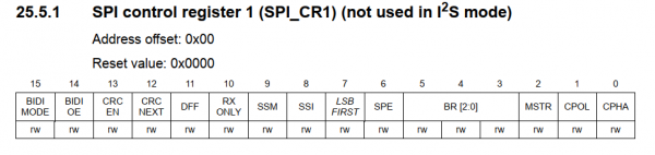
The BR bits set the frequency divider of the controller, thereby determining the frequency at which SPI will operate. The STM32 frequency will be 72 MHz, the LED driver, according to its datasheet, operates at a frequency of up to 25 MHz, thus, we need to divide by four (BR[2:0] = 001).
#define _SPI_CR1 0x00

#define BR_0        0x0008
#define BR_1        0x0010
#define BR_2        0x0020

_SPI2_ (_SPI_CR1) |= BR_0;// pclk/4
2. Set the CPOL and CPHA bits to determine the relationships between data transmission and clocking of the serial interface (see the diagram on page 240).
Since we are reading the datasheet here and not examining schematics, let's better study the textual description of the CPOL and CPHA bits on page 704 (SPI General Description):
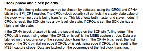
Clock signal phase and polarity.
Using the CPOL and CPHA bits of the SPI_CR1 register, you can programmatically select four variations of timing relationships. The CPOL bit (clock signal polarity) controls the state of the clock signal when data is not being transmitted. This bit governs the master and slave modes. If CPOL is reset, the SCK pin in idle mode is at a low level. If the CPOL bit is set, the SCK pin in idle mode is at a high level.
If the CPHA (Clock Phase) bit is set, the second edge of the SCK signal acts as the latch clock for the most significant bit (falling edge if CPOL is cleared, or rising edge if CPOL is set). Data is captured on the second clock edge. If the CPHA bit is cleared, the first edge of the SCK signal acts as the latch clock for the most significant bit (falling edge if CPOL is set, or rising edge if CPOL is cleared). Data is captured on the first clock edge.
Having absorbed this knowledge, we conclude that both bits must remain zeros since we want the SCK signal to stay low when not in use, while data is transmitted on the leading edge of the pulse (see Rising Edge in the DM634 datasheet).
By the way, here we first encountered a peculiarity of the terminology in ST datasheets: the phrase 'to reset a bit' is written to reset a bit, not to clear a bit, as, for example, in the case of Atmega.
3. Set the DFF bit to determine the 8-bit or 16-bit data block format.
I specifically took the 16-bit DM634 to avoid the hassle of transmitting 12-bit PWM data like with the DM633. It makes sense to set DFF to one:
#define DFF         0x0800

_SPI2_ (_SPI_CR1) |= DFF; // 16-bit mode
4. Configure the LSBFIRST bit in the SPI_CR1 register to determine the block format.
LSBFIRST, as its name suggests, configures the transmission to start with the least significant bit. However, the DM634 wants to receive data starting with the most significant bit. Therefore, we leave it cleared.
5. In hardware mode, if input from the NSS pin is required, apply a high signal to the NSS pin during the entire byte transmission sequence. In software mode, set the SSM and SSI bits in the SPI_CR1 register. If the NSS pin needs to be an output, only the SSOE bit must be set.
Set SSM and SSI to forget about the hardware mode of NSS:
#define SSI         0x0100
#define SSM         0x0200

_SPI2_ (_SPI_CR1) |= SSM | SSI; //enable software control of SS, SS high
6. The MSTR and SPE bits must be set (they remain set only if a high signal is applied to NSS).
These bits effectively designate our SPI as the master and enable it:
#define MSTR        0x0004
#define SPE         0x0040

_SPI2_ (_SPI_CR1) |= MSTR; //SPI master
//когда все готово, включаем SPI
_SPI2_ (_SPI_CR1) |= SPE;
SPI is configured, so let’s immediately write functions to send bytes to the driver. Let’s continue reading section 25.3.3 'Configuring SPI in master mode':
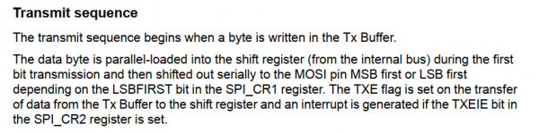
Data transmission order
Transmission begins when a byte is written to the Tx buffer.
The data byte is loaded into the shift register in parallel mode (from the internal bus) during the transmission of the first bit, after which it is sent out in serial. In MOSI mode, the first or last bit is sent forward depending on the LSBFIRST bit setting in the CPI_CR1 register. The TXE flag is set after data is transmitted. from the Tx buffer to the shift register., and an interrupt is generated if the TXEIE bit is set in the CPI_CR1 register.
I highlighted a few words in the translation to draw attention to a specific feature of SPI implementation in STM controllers. On the Atmega, the TXE flag (Tx Empty, Tx is empty and ready to accept data) is set only after the entire byte is sent outwards.. Here, this flag is set after the byte has been pushed into the internal shift register. Since it is pushed in all bits at once (in parallel), and then the data is transmitted sequentially, TXE is set before the byte is completely sent. This is important, as in the case of our LED driver, we need to toggle the LAT pin after sending all the data, meaning the TXE flag alone will not be sufficient.
This means we need another flag. Let's look at 25.3.7 – "Status Flags":

<…>

BUSY Flag
The BSY flag is set and reset hardware-wise (writing to it has no effect). The BSY flag indicates the state of the SPI communication layer.
It is reset:
when the transmission is completed (except for master mode if the transmission is continuous)
when SPI is disabled
when a master mode error occurs (MODF=1)
If the transmission is not continuous, the BSY flag is cleared between each data transmission.
Okay, useful. Now let's find out where the Tx buffer is located. To do this, we read the "SPI Data Register":
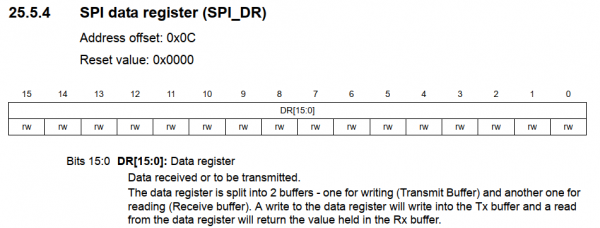
Bits 15:0 DR[15:0] Data Register
Received data or data to be transmitted.
The data register is divided into two buffers – one for writing (transmit buffer) and the other for reading (receive buffer). Writing to the data register writes to the Tx buffer, while reading from the data register returns the value contained in the Rx buffer.
Now for the status register, where the TXE and BSY flags can be found:
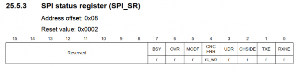
We write:
#define _SPI_DR  0x0C
#define _SPI_SR  0x08

#define BSY         0x0080
#define TXE         0x0002

void dm_shift16(uint16_t value)
{
    _SPI2_(_SPI_DR) = value; //send 2 bytes
    while (!(_SPI2_(_SPI_SR) & TXE)); //wait until they're sent
}
Since we need to transmit 16 times two bytes, based on the number of LED driver outputs, it looks something like this:
void sendLEDdata()
{
    LAT_low();
    uint8_t k = 16;
    do
    {   k--;
        dm_shift16(leds[k]);
    } while (k);

    while (_SPI2_(_SPI_SR) & BSY); // finish transmission

    LAT_pulse();
}
But for now, we don’t know how to toggle the LAT pin, so let’s go back to I/O.
Assigning pins
The registers in STM32F1 that are responsible for pin states are quite unusual. It’s clear that there are more of them than in Atmega, but they also differ from other STM chips. Section 9.1 General Description of GPIO:

Each general-purpose input/output port (GPIO) has two 32-bit configuration registers (GPIOx_CRL and GPIOx_CRH), two 32-bit data registers (GPIOx_IDR and GPIOx_ODR), a 32-bit set/reset register (GPIOx_BSRR), a 16-bit reset register (GPIOx_BRR), and a 32-bit lock register (GPIOx_LCKR).
They are unusual and also quite inconvenient since the first two registers contain 16 pins of the port scattered in a ‘four bits per brother’ format. That is, pins 0 through 7 reside in CRL, while the others are in CRH. Meanwhile, the other registers successfully accommodate bits for all port pins—often remaining half 'reserved.'
For simplicity, let's start at the end of the list.
We won’t need the lock register.
Set and reset registers are amusing because they partially duplicate each other: you can write everything only in BSRR, where the higher 16 bits reset the pin to zero and the lower bits set it to 1, or also use BRR, whose lower 16 bits only reset the pin. I prefer the second option. These registers are important as they provide atomic access to the pins:


Atomic set or reset
You do not need to disable interrupts when programming GPIOx_ODR at the bit level: you can modify one or several bits with a single atomic write operation to APB2. This is achieved by writing '1' to the set/reset register (GPIOx_BSRR or, for reset only, GPIOx_BRR) of the bit you want to change. Other bits will remain unchanged.
Data registers have quite descriptive names – IDR = Input Direction Register, input register; ODR = Output Direction Register, output register. In the current project, we won’t need them.
And finally, the control registers. Since we are interested in the pins of the second SPI, specifically PB13, PB14, and PB15, let's look directly at CRH:
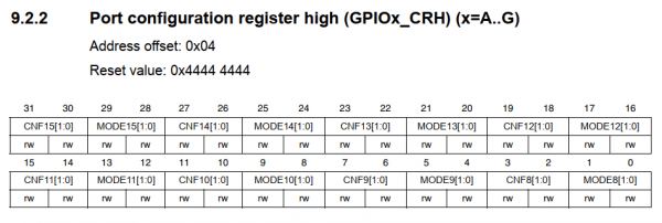
And we see that we need to write something to bits 20 through 31.
We have already discussed what we want from the pins, so I won’t include a screenshot here; I will just say that MODE sets the direction (input if both bits are set to 0) and the speed of the pin (we need 50MHz, which means both pins are at '1'), while CNF sets the mode: normal 'push-pull' – 00, 'alternative' – 10. By default, as we can see above, the third bottom bit (CNF0) is set for all pins, which places them in mode. floating input.
Since I plan to do something else with this chip, for simplicity, I have defined all possible values for MODE and CNF for both the lower and upper control registers.
So here it is.
#define CNF0_0 0x00000004
#define CNF0_1 0x00000008
#define CNF1_0 0x00000040
#define CNF1_1 0x00000080
#define CNF2_0 0x00000400
#define CNF2_1 0x00000800
#define CNF3_0 0x00004000
#define CNF3_1 0x00008000
#define CNF4_0 0x00040000
#define CNF4_1 0x00080000
#define CNF5_0 0x00400000
#define CNF5_1 0x00800000
#define CNF6_0 0x04000000
#define CNF6_1 0x08000000
#define CNF7_0 0x40000000
#define CNF7_1 0x80000000
#define CNF8_0 0x00000004
#define CNF8_1 0x00000008
#define CNF9_0 0x00000040
#define CNF9_1 0x00000080
#define CNF10_0 0x00000400
#define CNF10_1 0x00000800
#define CNF11_0 0x00004000
#define CNF11_1 0x00008000
#define CNF12_0 0x00040000
#define CNF12_1 0x00080000
#define CNF13_0 0x00400000
#define CNF13_1 0x00800000
#define CNF14_0 0x04000000
#define CNF14_1 0x08000000
#define CNF15_0 0x40000000
#define CNF15_1 0x80000000

#define MODE0_0 0x00000001
#define MODE0_1 0x00000002
#define MODE1_0 0x00000010
#define MODE1_1 0x00000020
#define MODE2_0 0x00000100
#define MODE2_1 0x00000200
#define MODE3_0 0x00001000
#define MODE3_1 0x00002000
#define MODE4_0 0x00010000
#define MODE4_1 0x00020000
#define MODE5_0 0x00100000
#define MODE5_1 0x00200000
#define MODE6_0 0x01000000
#define MODE6_1 0x02000000
#define MODE7_0 0x10000000
#define MODE7_1 0x20000000
#define MODE8_0 0x00000001
#define MODE8_1 0x00000002
#define MODE9_0 0x00000010
#define MODE9_1 0x00000020
#define MODE10_0 0x00000100
#define MODE10_1 0x00000200
#define MODE11_0 0x00001000
#define MODE11_1 0x00002000
#define MODE12_0 0x00010000
#define MODE12_1 0x00020000
#define MODE13_0 0x00100000
#define MODE13_1 0x00200000
#define MODE14_0 0x01000000
#define MODE14_1 0x02000000
#define MODE15_0 0x10000000
#define MODE15_1 0x20000000
Our pins are located on port B (base address – 0x40010C00), code:
#define _PORTB_(mem_offset) (*(volatile uint32_t *)(0x40010C00 + (mem_offset)))

#define _BRR  0x14
#define _BSRR 0x10
#define _CRL  0x00
#define _CRH  0x04

//используем стандартный SPI2: MOSI на B15, CLK на B13
//LAT пусть будет на неиспользуемом MISO – B14

//очищаем дефолтный бит, он нам точно не нужен
_PORTB_ (_CRH) &= ~(CNF15_0 | CNF14_0 | CNF13_0 | CNF12_0);

//альтернативные функции для MOSI и SCK
_PORTB_ (_CRH) |= CNF15_1 | CNF13_1;

//50 МГц, MODE = 11
_PORTB_ (_CRH) |= MODE15_1 | MODE15_0 | MODE14_1 | MODE14_0 | MODE13_1 | MODE13_0;
And accordingly, we can write defines for LAT, which will toggle the registers BRR and BSRR:
/*** LAT pulse – high, then low */
#define LAT_pulse() _PORTB_(_BSRR) = (1<<14); _PORTB_(_BRR) = (1<<14)

#define LAT_low() _PORTB_(_BRR) = (1<<14)
(LAT_low is just a matter of inertia, it's always been this way, so I’ll let it stay)
Now everything is great, except it doesn’t work. Because this is STM32, which saves electricity, we need to enable the clocking of the necessary peripherals.
Enabling clocking
The clock is controlled by the clocks, also known as Clock. And we may have already noticed the abbreviation RCC. Let’s look it up in the documentation: it stands for Reset and Clock Control.
As mentioned above, fortunately, the most complex part of the clocking topic has been done for us by the folks at STM, for which we are very thankful (I’ll link to , to understand how complicated it is). We only need the registers responsible for enabling the clocking of the peripherals (Peripheral Clock Enable Registers). First, let's find the base address of RCC, which is at the very beginning of the 'Memory Map':

#define _RCC_(mem_offset) (*(volatile uint32_t *)(0x40021000 + (mem_offset)))Then either click on the link to search something in the table or, much better, browse through the descriptions of the enabling registers from the sections about enable registers. Here we will find RCC_APB1ENR and RCC_APB2ENR:
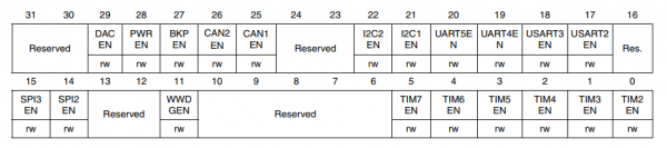
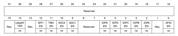
And in them, respectively, the bits that enable the clocking for SPI2, IOPB (I/O Port B), and alternative functions (AFIO).
#define _APB2ENR 0x18
#define _APB1ENR 0x1C

#define IOPBEN 0x0008
#define SPI2EN 0x4000
#define AFIOEN 0x0001

//включаем тактирование порта B и альт. функций
_RCC_(_APB2ENR) |= IOPBEN | AFIOEN;

//включаем  тактирование SPI2
_RCC_(_APB1ENR) |= SPI2EN;
The final code can be found .
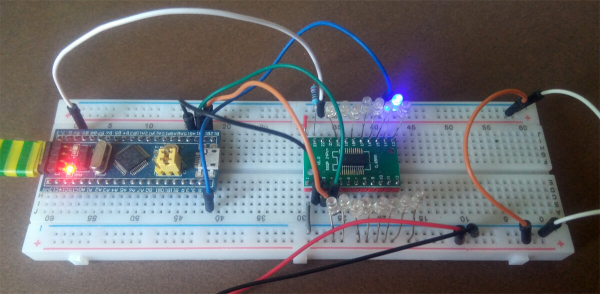
If there’s an opportunity and desire to test, connect DM634 like this: DAI to PB15, DCK to PB13, LAT to PB14. Power the driver from 5 volts, and do not forget to connect the grounds.
STM8 PWM
PWM on STM8
When I first planned this article, I decided to try mastering some functionality of an unfamiliar chip using only the datasheet as an example, so I wouldn't be a shoemaker without shoes. The STM8 was perfect for this: firstly, I had a couple of Chinese boards with STM8S103, and secondly, it's not very popular, which means the temptation to cheat and find solutions online is limited by the absence of those very solutions.
There is also a chip and , in the first one pinout and register addresses, in the second - everything else. The STM8 is programmed in C in a rather basic IDE .
Clocking and Input-Output
By default, the STM8 operates at a frequency of 2 MHz, which needs to be adjusted immediately.
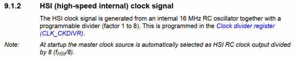
The HSI clock signal (High-Speed Internal)
The HSI clock signal comes from the internal 16-MHz RC generator with a programmable divider (from 1 to 8). It is set in the clock divider register (CLK_CKDIVR).
Note: at startup, the leading clock source is selected as the HSI RC generator with a divider of 8.
We find the register address in the datasheet, the description in the refman, and see that the register needs to be cleared:
#define CLK_CKDIVR *(volatile uint8_t *)0x0050C6

CLK_CKDIVR &= ~(0x18);
Since we are going to run PWM and connect LEDs, let's look at the pinout:
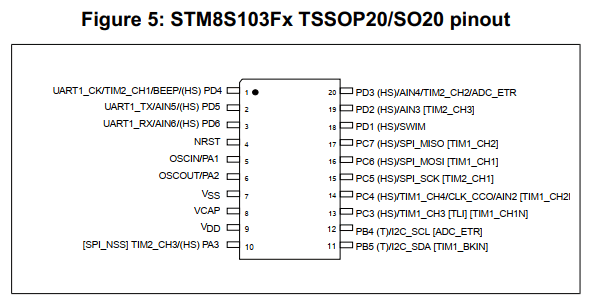
The chip is small, many functions are mapped to the same pins. What is in square brackets is 'alternative functionality', which can be switched by 'option bytes' (option bytes) - something like the fuses in Atmega. Their values can be changed programmatically, but it’s not necessary since the new functionality is activated only after a reset. It's simpler to use the ST Visual Programmer (which comes with Visual Develop), which can change these bytes. The pinout shows that outputs CH1 and CH2 of the first timer are hidden in square brackets; you need to set bits AFR1 and AFR0 in STVP, with the second one also moving output CH1 of the second timer from PD4 to PC5.
Thus, the LEDs will be controlled by 6 pins: PC6, PC7, and PC3 for the first timer, PC5, PD3, and PA3 for the second.
Configuring the input-output pins on the STM8 is simpler and more logical than on the STM32:
- the familiar DDR data direction register (Data Direction Register): 1 = output;
- the first control register CR1 sets the mode as 'push-pull' (1) or open-drain (0) when outputting; since I’m connecting the LEDs to the chip's cathodes, I leave this as zeros;
- the second control register CR2 sets the output speed: 1 = 10 MHz
#define PA_DDR     *(volatile uint8_t *)0x005002
#define PA_CR2     *(volatile uint8_t *)0x005004
#define PD_DDR     *(volatile uint8_t *)0x005011
#define PD_CR2     *(volatile uint8_t *)0x005013
#define PC_DDR     *(volatile uint8_t *)0x00500C
#define PC_CR2     *(volatile uint8_t *)0x00500E

PA_DDR = (1<<3); //output
PA_CR2 |= (1<<3); //fast
PD_DDR = (1<<3); //output
PD_CR2 |= (1<<3); //fast
PC_DDR = ((1<<3) | (1<<5) | (1<<6) | (1<<7)); //output
PC_CR2 |= ((1<<3) | (1<<5) | (1<<6) | (1<<7)); //fast
PWM Setup
First, let's clarify the terms:
- PWM Frequency – the frequency at which the timer ticks;
- Auto-reload, AR – the auto-reloaded value up to which the timer will count (pulse period);
- Update Event, UEV – an event that occurs when the timer reaches AR;
- PWM Duty Cycle – the PWM duty cycle, often referred to as 'duty ratio';
- Capture/Compare Value – the value for capture/comparison that the timer counts up to to perform an action (in the case of PWM, it inverts the output signal);
- Preload Value – the preloaded value. The compare value cannot change while the timer is counting, otherwise the PWM cycle will break. Therefore, new transmitted values are placed in a buffer and are retrieved when the timer reaches the end of the count and resets;
- Edge-aligned and Center-aligned modes – aligning at the edge and in the center, the same as Atmega's modes. Fast PWM and Phase-correct PWM.
- OCiREF, Output Compare Reference Signal – the reference output signal, which, in PWM mode, appears on the corresponding pin.
As is clear from the pinout, both timers – the first and the second – have PWM capabilities. Both are 16-bit, and the first has many additional features (notably, it can count both up and down). We need both to operate identically, so I decided to start with the inherently more limited second one to avoid accidentally using something that isn't available. A slight issue is that the description of PWM functionality for all timers is located in the reference manual in the chapter about the first timer (17.5.7 PWM Mode), so I have to keep jumping back and forth in the document.
The PWM on STM8 has a significant advantage over the PWM on Atmega:
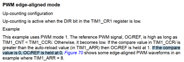
Edge-aligned PWM
Bottom-up counting configuration
Bottom-up counting is active when the DIR bit in the TIM_CR1 register is cleared.
Example
The example uses the first PWM mode. The PWM reference signal OCiREF is held high while TIM1_CNT < TIM1_CCRi. Otherwise, it takes a low level. If the compare value in the TIM1_CCRi register is greater than the auto-reload value (TIM1_ARR register), the OCiREF signal is held at 1. If the compare value is 0, OCiREF is held at zero.…
The STM8 timer during the update event first checks the compare value, and only then outputs the reference signal. In Atmega, the timer first fires and then compares, resulting in situations where the compare value == 0 As a result, we have a needle that we need to somehow deal with (for example, by programmatically inverting the logic).
So, what we want to do: 8-bit PWM (AR == 255), counting from bottom to top, aligning by boundary. Since the bulbs are connected to the chip via cathodes, PWM should output 0 (LED is on) until the compare value and 1 after.
We have already read about some PWM mode, so we find the required register of the second timer by searching in the reference manual for this phrase (18.6.8 – TIMx_CCMR1):

110: First PWM mode – when counting from bottom to top, the first channel is active while TIMx_CNT < TIMx_CCR1. Otherwise, the first channel is inactive. [further in the document, there is an erroneous copy-paste from timer 1]
111: Second PWM mode – when counting from bottom to top, the first channel is inactive while TIMx_CNT < TIMx_CCR1. Otherwise, the first channel is active.
Since the LEDs are connected to the MCU via cathodes, the second mode suits us (the first one also works, but we don't know that yet).
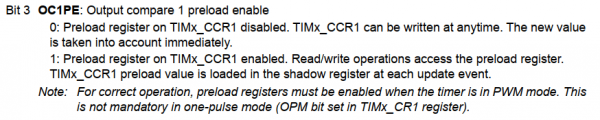
Bit 3 OC1PE: Enable preload for output 1
0: Preload register on TIMx_CCR1 is disabled. Writing to TIMx_CCR1 can be done at any time. The new value takes effect immediately.
1: Preload register on TIMx_CCR1 is enabled. Read/write operations access the preload register. The preloaded value of TIMx_CCR1 is loaded into the shadow register at each update event.
*Note: For proper operation of the PWM mode, preload registers must be enabled. This is not necessary in single signal mode (bit OPM is set in register TIMx_CR1).
Okay, let's enable everything needed for three channels of the second timer:
#define TIM2_CCMR1 *(volatile uint8_t *)0x005307
#define TIM2_CCMR2 *(volatile uint8_t *)0x005308
#define TIM2_CCMR3 *(volatile uint8_t *)0x005309

#define PWM_MODE2   0x70 //PWM mode 2, 0b01110000
#define OCxPE       0x08 //preload enable

TIM2_CCMR1 = (PWM_MODE2 | OCxPE);
TIM2_CCMR2 = (PWM_MODE2 | OCxPE);
TIM2_CCMR3 = (PWM_MODE2 | OCxPE);
AR consists of two 8-bit registers, it's straightforward here:
#define TIM2_ARRH  *(volatile uint8_t *)0x00530F
#define TIM2_ARRL  *(volatile uint8_t *)0x005310

TIM2_ARRH = 0;
TIM2_ARRL = 255;
The second timer can only count up, aligning by boundary; nothing needs to be changed. We'll set the frequency divider to, say, 256. The divider for the second timer is set in the TIM2_PSCR register and represents a power of two:
#define TIM2_PSCR  *(volatile uint8_t *)0x00530E

TIM2_PSCR = 8;
Now we need to enable the outputs and the second timer itself. The first task is solved by the registers Capture/Compare Enable: there are two of them, with three channels spread asymmetrically across them. Here we can also find out that the signal polarity can be changed, meaning we could have used PWM Mode 1. We write:
#define TIM2_CCER1 *(volatile uint8_t *)0x00530A
#define TIM2_CCER2 *(volatile uint8_t *)0x00530B

#define CC1E  (1<<0) // CCER1
#define CC2E  (1<<4) // CCER1
#define CC3E  (1<<0) // CCER2

TIM2_CCER1 = (CC1E | CC2E);
TIM2_CCER2 = CC3E;
And finally, we start the timer in the TIMx_CR1 register:
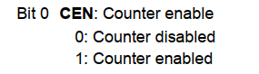
#define TIM2_CR1   *(volatile uint8_t *)0x005300

TIM2_CR1 |= 1;
We will write a simple analog for AnalogWrite() that will send the actual values for comparison to the timer. The registers are predictably named Capture/Compare registers, two for each channel: the lower 8 bits in TIM2_CCRxL and the upper in TIM2_CCRxH. Since we set up an 8-bit PWM, it's sufficient to only write the lower bits:
#define TIM2_CCR1L *(volatile uint8_t *)0x005312
#define TIM2_CCR2L *(volatile uint8_t *)0x005314
#define TIM2_CCR3L *(volatile uint8_t *)0x005316

void setRGBled(uint8_t r, uint8_t g, uint8_t b)
{
    TIM2_CCR1L = r;
    TIM2_CCR2L = g;
    TIM2_CCR3L = b;
}
The attentive reader will notice that we ended up with a slightly flawed PWM, unable to produce 100% duty cycle (with a maximum value of 255, the signal inverts for one timer cycle). This doesn't matter for LEDs, but the careful reader can already guess how to fix it.
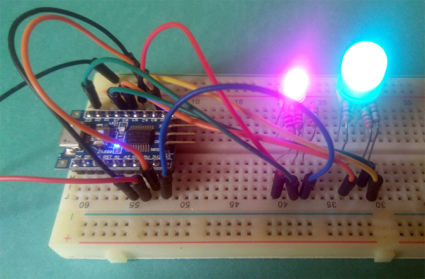
The PWM on the second timer works, let's move to the first one.
The first timer has exactly the same bits in the same registers (the bits that were 'reserved' in the second timer are actively used in the first for various advanced functions). Therefore, it's enough to find the addresses of these registers in the datasheet and copy the code. Also, change the frequency divider value, since the first timer requires not a power of two, but an exact 16-bit value in two registers. Prescaler High and Low. We do everything and… the first timer does not work. What's the issue?
The problem can only be solved by reviewing the entire section on the control registers of timer 1, where we look for the one not present in the second timer. It will be found: 17.7.30 Break register (TIM1_BKR), which has such a bit:

Enable the main output
#define TIM1_BKR   *(volatile uint8_t *)0x00526D

TIM1_BKR = (1<<7);
Now everything is definitely set, the code .
STM8 Multiplex
Multiplexing on STM8
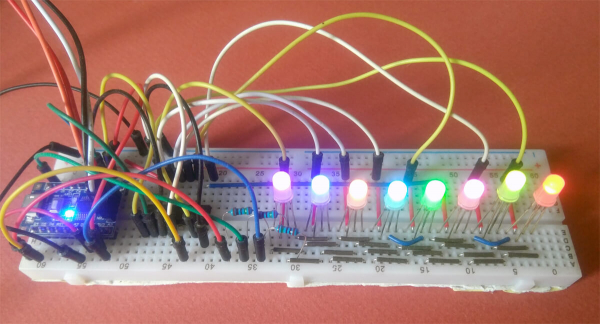
The third mini-project involves connecting eight RGB LEDs to the second timer in PWM mode and making them display different colors. At its core is the concept of LED multiplexing, where if you turn the LEDs on and off very quickly, it will seem to us that they are constantly lit (persistence of vision, the inertia of visual perception). At one time, I did .
The working algorithm looks like this:
- connect the anode of the first RGB LED;
- light it up by sending the appropriate signals to the cathodes;
- wait for the end of the PWM cycle;
- connect the anode of the second RGB LED;
- light it up…
And so on. Of course, for smooth operation, the connection of the anode and the 'lighting' of the LED must occur simultaneously. Well, or almost. In any case, we need to write code that will output values on the three channels of the second timer, changing them upon reaching UEV and simultaneously switching the currently active RGB LED.
Since the LED switching is done automatically, we need to create a 'video memory' from which the interrupt handler will obtain data. This is a simple array:
uint8_t colors[8][3];To change the color of a specific LED, it is enough to write the desired values into this array. The variable responsible for the number of the active LED will be
uint8_t cnt;Demux
For proper multiplexing, we will oddly need a CD74HC238 demultiplexer. A demultiplexer is a chip that implements the operator <<. Through three input pins (bits 0, 1, and 2), we feed it a three-bit number X, and it activates the output number (1<<X). The other chip inputs are used to scale the whole setup. This chip is necessary not only to reduce the number of pins occupied on the microcontroller but also for safety—to avoid accidentally turning on more LEDs than allowed and burning the MCU. The chip costs very little, so it's worth keeping in your toolkit.
CD74HC238 will be responsible for supplying voltage to the anode of the required LED. In a full multiplexing setup, it would supply voltage to the column via a P-MOSFET, but in this demo, we can connect it directly, as it draws 20 mA, according to absolute maximum ratings in the datasheet. From , we will need the pinout and this cheat sheet:
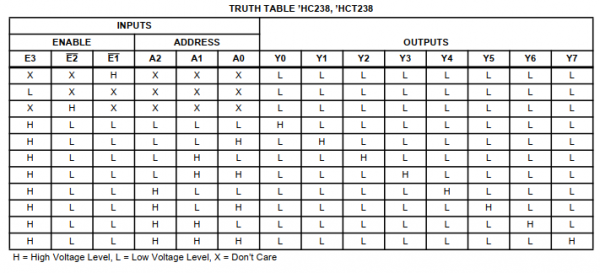
H = high voltage level, L = low voltage level, X = don't care
Connect E2 and E1 to ground, E3, A0, A1, and A3 to pins PD5, PC3, PC4, and PC5 of STM8. Since the table above contains both low and high levels, configure these pins as push-pull outputs.
PWM
PWM on the second timer is set up just like in the previous case, with two differences:
First, we need to enable the interrupt on Update Event (UEV), which will call the function that switches the active LED. This is done by changing the bit Update Interrupt Enable in the register with a telling name

Interrupt Enable Register
#define TIM2_IER   *(volatile uint8_t *)0x005303

//enable interrupt
TIM2_IER = 1;
The second difference is related to the phenomenon of multiplexing known as ghosting – parasitic glow of the diodes. In our case, it can appear because the timer, triggering an interrupt on UEV, continues ticking, and the interrupt handler does not manage to switch the LED before the timer starts writing something to the outputs. To combat this, we will need to invert the logic (0 = maximum brightness, 255 = nothing is lit) and avoid extreme duty cycle values. That is, we need to ensure that after UEV, the LEDs completely turn off for one PWM cycle.
Change polarity:
//set polarity
    TIM2_CCER1 |= (CC1P | CC2P);
    TIM2_CCER2 |= CC3P;
Avoid setting r, g, and b to 255 and don’t forget to invert them when used.
Interrupts
The essence of an interrupt is that under certain circumstances, the chip stops executing the main program and calls an external function. Interrupts occur due to external or internal influences, including from a timer.
When we first created the project in ST Visual Develop, in addition to main.c we received a window with a mysterious file stm8_interrupt_vector.c, automatically included in the project. This file is linked to a function for each interrupt NonHandledInterrupt. We need to link our function to the required interrupt.
The datasheet contains a table of interrupt vectors, where we find the necessary ones:

13 TIM2 update/overflow
14 TIM2 capture/comparison
We need to change the LED at UEV, so we need interrupt No. 13.
Accordingly, first, in the file stm8_interrupt_vector.c change the name of the function responsible for interrupt No. 13 (IRQ13) from the default to our own:
{0x82, TIM2_Overflow}, /* irq13 */Secondly, we will need to create a file main.h with the following content:
#ifndef __MAIN_H
#define __MAIN_H

@far @interrupt void TIM2_Overflow (void);
#endif
And finally, we need to write this function in our main.c:
@far @interrupt void TIM2_Overflow (void)
{
    PD_ODR &= ~(1<<5); // disable the demultiplexer
    PC_ODR = (cnt<<3); // write the new value to the demultiplexer
    PD_ODR |= (1<<5); // enable the demultiplexer

    TIM2_SR1 = 0; // reset Update Interrupt Pending flag

    cnt++;
    cnt &= 7; // shift the LED counter

    TIM2_CCR1L = ~colors[cnt][0]; // send inverted values to the buffer
    TIM2_CCR2L = ~colors[cnt][1]; // for the next PWM cycle
    TIM2_CCR3L = ~colors[cnt][2]; //

    return;
}
Now we need to enable interrupts. This is done with the assembler command rim – you'll have to look for it in :
//enable interrupts
_asm("rim");
The other assembler command – sim – disables interrupts. They need to be turned off while writing new values to the 'video memory' so that an untimely interrupt does not corrupt the array.
The entire code is available on .
If this article helps even one person, then I have written it for a reason. I welcome comments and feedback, and I will do my best to respond to everyone.
Source: habr.com
