

In light of the approaching barrier in chip manufacturing, which is the inability to continue scaling down the process, multi-die packaging of chips comes to the forefront. The performance of future processors will be measured by the complexity, or better yet, the richness of solutions. The more functions are placed on a small processor chip, the more powerful and efficient the entire platform will be. At the same time, the processor itself will represent a platform made up of many heterogeneous chips connected by a high-speed bus, which will be at least as good (in terms of speed and consumption) as if it were a single monolithic chip. In other words, the processor will act as both the motherboard and a set of expansion cards, including memory, peripherals, and more.
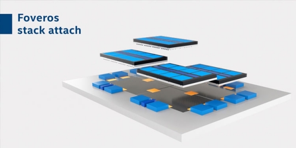
Intel has already demonstrated the implementation of two proprietary technologies for spatial packaging of heterogeneous chips into a single package. These are the EMIB and . The first represents embedded interface bridges in the 'mounting' substrate for horizontal chip arrangement, while the second is a three-dimensional or stacked arrangement of chips using, among other things, through vertical metalization channels, TSVs. With the EMIB technology, the company is producing Stratix X generation FPGAs and hybrid Kaby Lake G processors, while the Foveros technology is set to be implemented in commercial products in the second half of this year. For example, notebook processors Lakefield will be produced using it.
Undoubtedly, Intel will not stop here and will continue to actively develop technologies for advanced chip packaging. Competitors are doing the same. Both and Samsung are developing technologies for the spatial arrangement of chips (chiplets) and intend to further pull the blanket of new opportunities towards themselves.
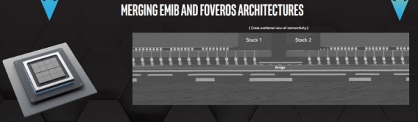
Recently, at the SEMICON West conference, Intel once again , that its technologies for multi-chip packaging are progressing well. Three technologies have been showcased at the event, which will be implemented in the near future. It should be noted that none of these three technologies will become industry standards. All developments are kept by Intel for itself and will only be provided to customers under contract manufacturing.
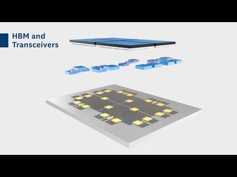
The first of the three new technologies for spatial chiplet packaging is Co-EMIB. This is a combination of the low-cost EMIB bridge technology with Foveros chiplets. The Foveros multi-chip stack designs can be connected with horizontal EMIB links into complex systems without compromising bandwidth and performance. Intel claims that the latency and bandwidth of all multi-level interfaces will be no worse than in a monolithic chip. In fact, due to the extreme density of heterogeneous crystals, the overall performance and energy efficiency of the solution and interfaces will be even higher than that of a monolithic solution.
For the first time, the Co-EMIB technology may be implemented for the production of Intel's hybrid processors for the Aurora supercomputer, expected to be delivered by the end of 2021 (a joint project of Intel and Cray). A prototype of the processor was showcased at SEMICON West as a stack of 18 small crystals on one large crystal (Foveros), with pairs connected horizontally via EMIB.
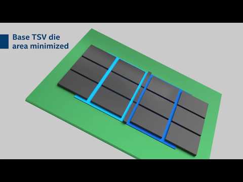
The second of the three new technologies for spatial chip packaging by Intel is called Omni-Directional Interconnect (ODI). This technology involves the use of EMIB and Foveros interfaces for both horizontal and vertical electrical connections between crystals. The need to highlight ODI separately arose from the fact that the company implemented power delivery to chiplets in the stack using vertical TSV interconnections. This approach will enable efficient power distribution. At the same time, the resistance of the 70-micron TSV channels for power delivery is significantly reduced, which will decrease the number of channels needed for power supply and free up area on the chip for transistors (for example).
Finally, Intel introduced the inter-crystal interface called MDIO as the third technology for spatial packaging. This is an Advanced Interface Bus (AIB) configured as a physical layer for inter-crystal signal exchange. Strictly speaking, this is the second generation of the AIB bus, which Intel is developing under DARPA's request. The first generation of AIB was unveiled in 2017, capable of transmitting data at a rate of 2 Gbps per contact. The MDIO bus will provide exchanges at a speed of 5.4 Gbps. This link will compete with the TSMC LIPINCON bus. While LIPINCON has a higher exchange speed of 8 Gbps, the Intel MDIO boasts a greater density of gigabytes per millimeter: 200 versus 67, thus Intel claims a development that is as good as that of its competitor.
Source: 3dnews.ru
