

Norwegian startup Lace Lithography, supported by Microsoft, raised $40 million in its first funding round to develop a lithographic scanner that uses a helium atom beam for processing silicon wafers. The company claims its technology will enable the creation of chip elements that are ten times smaller than existing lithography systems, with a beam width of just 0.1 nm — ASML's EUV scanners use radiation with a wavelength of 13.5 nm.
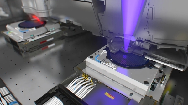
The advantage of Lace's system is that atoms do not have a diffraction limit, whereas photonic lithography, including EUV systems from ASML, is limited by the wavelength of the light used. As chip manufacturers shrink the sizes of elements, they rely on increasingly complex multilayer patterning methods to overcome this limitation, but Lace adopts a different approach by replacing photons with neutral helium atoms and a beam width roughly equal to that of a hydrogen atom.
Lace describes its systems as BEUV, or Beyond-EUV. Lace's CEO and co-founder Bodil Holst stated that the company's developed technology will allow chip manufacturers to print wafers with 'ultimately atomic resolution.' John Petersen, the chief scientist for lithography at Imec, believes this approach could reduce transistors and other elements by an order of magnitude to an 'almost unimaginable' degree.
Lace has joined the growing number of startups developing alternatives to ASML's advanced lithography. American companies Substrate and xLight are developing particle accelerator-based light sources for EUV or X-ray lithography, with xLight receiving $150 million in U.S. government funding. Canon delivered its first tool for nanoimprint lithography to the Texas Institute of Electronics as early as September 2024, while Chinese company Prinano recently introduced its own nanoimprint lithography system to the domestic market.
However, Lace's approach differs from all these companies. While Substrate and xLight still utilize photons, Lace completely abandons electromagnetic radiation. Although Lace has already created prototypes of the system, the gap between the lab and production remains as vast as ever. Currently, the company plans to deploy a test stand at a pilot facility by 2029, while the timeline for transitioning to mass production has yet to be announced.
It is worth noting that ASML spent decades and billions of dollars turning EUV lithography from a research concept into a commercial product. Currently, Lace employs over 50 people in Norway, Spain, the UK, and the Netherlands, and the company first presented initial results of its research at the SPIE Advanced Lithography + Patterning conference in 2026.
Source:
Source: 3dnews.ru
