The further development of microelectronics cannot be imagined without the improvement of semiconductor production technologies. To expand the boundaries and learn how to produce ever smaller elements on crystals, new technologies and new tools are needed. One of these technologies could be a breakthrough development by American scientists.

A team of researchers from the Argonne National Laboratory of the US Department of Energy a new technique for creating and etching the thinnest films on the surface of crystals. Potentially, this could lead to the production of chips with a smaller scale of technological norms than today and in the near future. The publication about the study is published in the journal Chemistry of Materials.
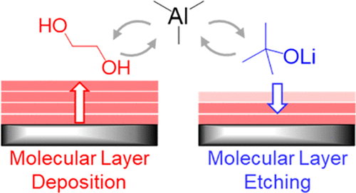
The proposed technique resembles the traditional process and etching, but instead of inorganic films, the new technology creates and works with organic films. Actually, by analogy, the new technology is called molecular layer deposition (MLD, molecular layer deposition) and molecular layer etching (MLE, molecular layer etching).
As in the case of atomic layer etching, the MLE method uses gas treatment in a crystal surface chamber with films of an organic-based material. The crystal is cyclically treated with two different gases alternately until the film is thinned to a predetermined thickness.
Chemical processes are subject to the laws of self-regulation. This means that layer after layer is removed evenly and in a controlled manner. If you use photomasks, you can reproduce the topology of the future chip on the chip and etch the pattern with the highest accuracy.

In the experiment, scientists used a gas containing lithium salts and a gas based on trimethylaluminum for molecular etching. During the etching process, the lithium compound reacted with the surface of the alucone film in such a way that lithium was deposited on the surface and destroyed the chemical bond in the film. Then trimethylaluminum was supplied, which removed the film layer with lithium, and so on in turn until the film was reduced to the desired thickness. Good controllability of the process, scientists believe, may allow the proposed technology to push the development of semiconductor production.
Source: 3dnews.ru


