

As has been repeatedly reported, something needs to be done with a transistor smaller than 5 nm. Today, chip manufacturers are producing the most advanced solutions using vertical FinFET gates. FinFET transistors can still be produced using 5nm and 4nm process technology (whatever these standards mean), but already at the production stage of 3nm semiconductors, FinFET structures stop working as they should. The gates of the transistors are too small, and the control voltage is not low enough for the transistors to continue their function as gates in integrated circuits. Therefore, the industry and, in particular, Samsung, starting from the 3-nm process technology, will switch to the manufacture of transistors with ring or GAA (Gate-All-Around) gates. With a fresh press release, Samsung just presented a visual infographic about the structure of new transistors and the benefits of using them.
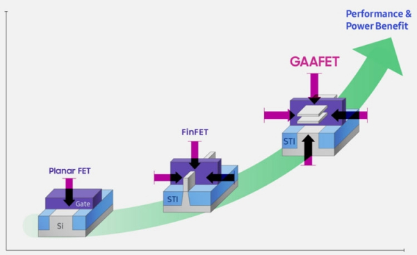
As shown in the illustration above, as manufacturing standards declined, gates went from planar structures that could control a single area under the gate to vertical channels surrounded by a gate on three sides, and finally closer to transition to channels surrounded by gates from all four sides. All this path was accompanied by an increase in the gate area around the controlled channel, which made it possible to reduce the power supply of transistors without compromising the current characteristics of the transistors, therefore, leading to an increase in transistor performance and a decrease in leakage currents. GAA transistors in this regard will be a new crown of creation and at the same time will not require significant alteration of classic CMOS processes.
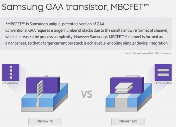
Gate-surrounded channels can be produced both in the form of thin bridges (nanowires) and in the form of wide bridges or nanopages. Samsung announces its choice in favor of nanopages and declares that it is protected by patents, although it developed all these structures while still in alliance with IBM and other companies, such as AMD. New Samsung transistors will not be called GAA, but by the proprietary name MBCFET (Multi Bridge Channel FET). Wide channel pages will provide significant currents that are difficult to achieve with nanowire channels.
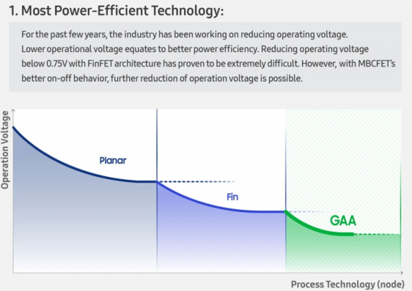
The transition to ring gates will also increase the energy efficiency of new transistor structures. This means that the supply voltage of the transistors can be reduced. For FinFET structures, the company calls 0,75 V a conditional power reduction threshold. Switching to MBCFET transistors will lower this limit even lower.
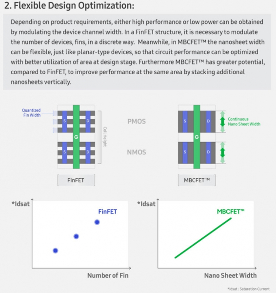
The company calls the extraordinary flexibility of solutions the next advantage of MBCFET transistors. So, if the characteristics of FinFET transistors at the production stage can only be controlled discretely, laying in the project a certain number of edges for each transistor, then designing circuits with MBCFET transistors will resemble the finest tuning for each project. And it will be very easy to do: it will be enough to choose the required width of nanopage channels, and this parameter can be changed linearly.
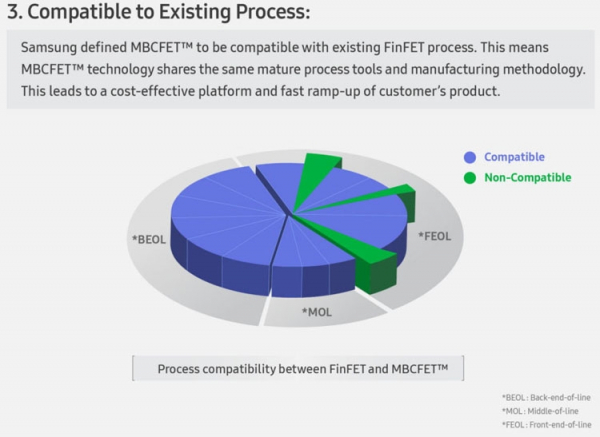
For the production of MBCFET transistors, as mentioned above, the classic CMOS process technology and factory-installed industrial equipment will do without significant changes. Only the stage of processing silicon wafers will require a little refinement, which is quite understandable, and that's it. From the side of the contact groups and metallization layers, you don’t even have to change anything.
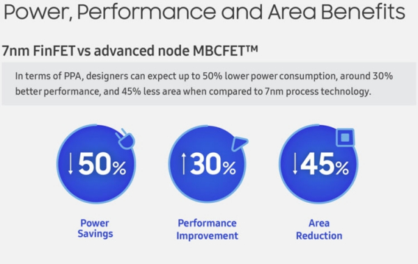
Samsung concludes for the first time with a qualitative characterization of the improvements that the transition to the 3nm process and MBCFETs will bring with it (to be clear, Samsung does not explicitly talk about the 3nm process, but it previously reported that the 4nm process will still use FinFET transistors). So, compared to the 7nm FinFET process technology, the transition to new standards and MBCFET will provide a 50% reduction in consumption, a 30% increase in performance, and a reduction in chip area by 45%. Not "or, or", namely in the aggregate. When will it happen? It may well be that by the end of 2021.
Source: 3dnews.ru
